SNVSBL0A November 2020 – December 2021 TPS7H4010-SEP
PRODUCTION DATA
- 1 Features
- 2 Applications
- 3 Description
- 4 Revision History
- 5 Pin Configuration and Functions
- 6 Specifications
-
7 Detailed Description
- 7.1 Overview
- 7.2 Functional Block Diagram
- 7.3
Feature Description
- 7.3.1 Synchronous Step-Down Regulator
- 7.3.2 Auto Mode and FPWM Mode
- 7.3.3 Fixed-Frequency Peak Current-Mode Control
- 7.3.4 Adjustable Output Voltage
- 7.3.5 Enable and UVLO
- 7.3.6 Internal LDO, VCC_UVLO, and BIAS Input
- 7.3.7 Soft Start and Voltage Tracking
- 7.3.8 Adjustable Switching Frequency
- 7.3.9 Frequency Synchronization and Mode Setting
- 7.3.10 Internal Compensation and CFF
- 7.3.11 Bootstrap Capacitor and VBOOT-UVLO
- 7.3.12 Power-Good and Overvoltage Protection
- 7.3.13 Overcurrent and Short-Circuit Protection
- 7.3.14 Thermal Shutdown
- 7.4 Device Functional Modes
-
8 Application and Implementation
- 8.1 Application Information
- 8.2
Typical Application
- 8.2.1 Design Requirements
- 8.2.2
Detailed Design Procedure
- 8.2.2.1 Output Voltage Setpoint
- 8.2.2.2 Switching Frequency
- 8.2.2.3 Input Capacitors
- 8.2.2.4 Inductor Selection
- 8.2.2.5 Output Capacitor Selection
- 8.2.2.6 Feed-Forward Capacitor
- 8.2.2.7 Bootstrap Capacitors
- 8.2.2.8 VCC Capacitor
- 8.2.2.9 BIAS
- 8.2.2.10 Soft Start
- 8.2.2.11 Undervoltage Lockout Setpoint
- 8.2.2.12 PGOOD
- 8.2.3 Application Curves
- 9 Power Supply Recommendations
- 10Layout
- 11Device and Documentation Support
- 12Mechanical, Packaging, and Orderable Information
Package Options
Refer to the PDF data sheet for device specific package drawings
Mechanical Data (Package|Pins)
- RNP|30
- KGD|0
Thermal pad, mechanical data (Package|Pins)
- RNP|30
Orderable Information
7.3.6 Internal LDO, VCC_UVLO, and BIAS Input
The TPS7H4010-SEP integrates an internal LDO, generating VCC voltage for control circuitry and MOSFET drivers. The VCC pin must have a 1-µF to 4.7-µF bypass capacitor placed as close as possible to the pin and properly grounded. Do not load the VCC pin or short it to ground during operation. Shorting VCC pin to ground during operation may damage the device.
The UVLO on VCC voltage, VCC_UVLO, turns off the regulation when VCC voltage is too low. It prevents the TPS7H4010-SEP from operating until the VCC voltage is enough for the internal circuitry. Hysteresis on VCC_UVLO prevents the part from turning off during power up if VIN droops due to input current demands. The LDO generates VCC voltage from one of the two inputs: the supply voltage VIN, or the BIAS input. When BIAS is tied to ground, the LDO input is VIN. When BIAS is tied to a voltage higher than 3.3 V, the LDO input is VBIAS. BIAS voltage must be lower than both VIN and 18 V.
The BIAS input is designed to reduce the LDO power loss. The LDO power loss is:
The higher the difference between the input and output voltages of the LDO, the more loss occurs to supply the same LDO output current. The BIAS input provides an option to supply the LDO with a lower voltage than VIN, to reduce the difference of the input and output voltages of the LDO and reduce power loss. For example, if the LDO current is 10 mA at a certain frequency with VIN = 24 V and VOUT = 5 V. The LDO loss with BIAS tied to ground is equal to 10 mA × (24 V – 3.27 V) = 207.3 mW, while the loss with BIAS tied to VOUT is equal to 10 mA × (5 – 3.27) = 17.3 mW.
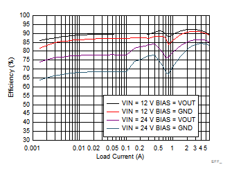
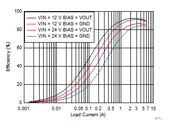
The efficiency improvement is more significant at light and mid loads because the LDO loss is a higher percentage in the total loss. The improvements is more significant with higher switching frequency because the LDO current is higher at higher switching frequency. The improvement is more significant when VIN » VOUT because the voltage difference is higher.
Figure 7-6 and Figure 7-7 show efficiency improvement with bias tied to VOUT in a VOUT = 5 V and fSW = 2200 kHz application, in auto mode and FPWM mode, respectively.

| VOUT = 5 V | fSW = 2200 kHz | Auto Mode |

| VOUT = 5 V | fSW = 2200 kHz | FPWM Mode |
TI recommends tying the BIAS pin to VOUT when VOUT is equal to or greater than 3.3 V and no greater than 18 V. Tie the BIAS pin to ground when not in use. A ceramic capacitor, CBIAS, can be used from the BIAS pin to ground for bypassing. If VOUT has high frequency noise or spikes during transients or fault conditions, a resistor (1 to 10 Ω) connected between VOUT to BIAS can be used together with CBIAS for filtering.
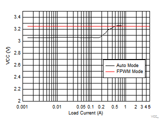
The VCC voltage is typically 3.27 V. When the TPS7H4010-SEP is operating in PFM mode with frequency foldback, VCC voltage is reduced to 3.1 V (typical) to further decrease the quiescent current and improve efficiency at very light loads. Figure 7-8 shows an example of VCC voltage change with mode change.

| VOUT = 5 V | fSW = 500 kHz | VIN = 12 V |
VCC voltage has an internal UVLO threshold, VCC_UVLO. When VCC voltage is higher than VCC_UVLO rising threshold, the device is active and in normal operation if VEN > VEN_VOUT_H. If VCC voltage droops below VCC_UVLO falling threshold, the VOUT is shut down.