SNVSBL0A November 2020 – December 2021 TPS7H4010-SEP
PRODUCTION DATA
- 1 Features
- 2 Applications
- 3 Description
- 4 Revision History
- 5 Pin Configuration and Functions
- 6 Specifications
-
7 Detailed Description
- 7.1 Overview
- 7.2 Functional Block Diagram
- 7.3
Feature Description
- 7.3.1 Synchronous Step-Down Regulator
- 7.3.2 Auto Mode and FPWM Mode
- 7.3.3 Fixed-Frequency Peak Current-Mode Control
- 7.3.4 Adjustable Output Voltage
- 7.3.5 Enable and UVLO
- 7.3.6 Internal LDO, VCC_UVLO, and BIAS Input
- 7.3.7 Soft Start and Voltage Tracking
- 7.3.8 Adjustable Switching Frequency
- 7.3.9 Frequency Synchronization and Mode Setting
- 7.3.10 Internal Compensation and CFF
- 7.3.11 Bootstrap Capacitor and VBOOT-UVLO
- 7.3.12 Power-Good and Overvoltage Protection
- 7.3.13 Overcurrent and Short-Circuit Protection
- 7.3.14 Thermal Shutdown
- 7.4 Device Functional Modes
-
8 Application and Implementation
- 8.1 Application Information
- 8.2
Typical Application
- 8.2.1 Design Requirements
- 8.2.2
Detailed Design Procedure
- 8.2.2.1 Output Voltage Setpoint
- 8.2.2.2 Switching Frequency
- 8.2.2.3 Input Capacitors
- 8.2.2.4 Inductor Selection
- 8.2.2.5 Output Capacitor Selection
- 8.2.2.6 Feed-Forward Capacitor
- 8.2.2.7 Bootstrap Capacitors
- 8.2.2.8 VCC Capacitor
- 8.2.2.9 BIAS
- 8.2.2.10 Soft Start
- 8.2.2.11 Undervoltage Lockout Setpoint
- 8.2.2.12 PGOOD
- 8.2.3 Application Curves
- 9 Power Supply Recommendations
- 10Layout
- 11Device and Documentation Support
- 12Mechanical, Packaging, and Orderable Information
Package Options
Refer to the PDF data sheet for device specific package drawings
Mechanical Data (Package|Pins)
- RNP|30
- KGD|0
Thermal pad, mechanical data (Package|Pins)
- RNP|30
Orderable Information
8.2.2.4 Inductor Selection
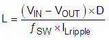
The first criterion for selecting an output inductor is the inductance. In most buck converters, this value is based on the desired peak-to-peak ripple current in the inductor, ILripple. An inductance that gives a ripple current of 10% to 30% of the maximum output current (6 A) is a good starting point. The inductance can be calculated from Equation 26:
where
- ILripple = (0.1 to 0.3) × IL_MAX
- IL_MAX = 6 A for TPS7H4010-SEP
- D = VOUT / VIN
Selected ILripple is between 10% to 30% of the rated current of the device.
As with switching frequency, the selection of the inductor is a tradeoff between size, cost, and performance. Higher inductance gives lower ripple current and hence lower output voltage ripple. With peak current mode control, the current ripple is the input signal to the control loop. A certain amount of ripple current is needed to maintain the signal-to-noise ratio of the control loop. Within the same series (same size/height), a larger inductance will have a higher series resistance (ESR). With similar ESR, size and/or height will be greater. Larger inductance also has slower current slew rate during large load transients.
Lower inductance usually results in a smaller, less expensive component; however, the current ripple will be higher, thus more output capacitor is needed to maintain the same amount of output voltage ripple. The RMS current is higher with the same load current due to larger ripple. The switching loss is higher because the switch current, which is the peak current, is higher when the HS switch turns off and LS switch turns on. Core loss of the inductor is also larger with higher ripple. Core loss needs to be considered, especially with higher switching frequencies. Check the ripple current over VIN_MIN to VIN_MAX range to make sure current ripple is reasonable over entire supply voltage range.
For applications with large VOUT and typical VOUT / VIN > 50%, sub-harmonic oscillation can be a concern in peak current-mode-controlled buck converters. Select inductance so that
where
- N = 3.6 with TPS7H4010-SEP
The second criterion is inductor saturation current rating. Because the maximum inductor current is limited by the high-side switch current limit, it is advised to select an inductor with a saturation current higher than the ILIMIT-HS. TI recommends selection of soft saturation inductors. A power inductor could be the major source of radiated noise. When EMI is a concern in the application, select a shielded inductor, if possible.
For this design, 20% ripple of 6 A yields 4.86-µH inductance. A 4.7-µH inductor is selected, which gives 21% ripple current.