SNVSBL0A November 2020 – December 2021 TPS7H4010-SEP
PRODUCTION DATA
- 1 Features
- 2 Applications
- 3 Description
- 4 Revision History
- 5 Pin Configuration and Functions
- 6 Specifications
-
7 Detailed Description
- 7.1 Overview
- 7.2 Functional Block Diagram
- 7.3
Feature Description
- 7.3.1 Synchronous Step-Down Regulator
- 7.3.2 Auto Mode and FPWM Mode
- 7.3.3 Fixed-Frequency Peak Current-Mode Control
- 7.3.4 Adjustable Output Voltage
- 7.3.5 Enable and UVLO
- 7.3.6 Internal LDO, VCC_UVLO, and BIAS Input
- 7.3.7 Soft Start and Voltage Tracking
- 7.3.8 Adjustable Switching Frequency
- 7.3.9 Frequency Synchronization and Mode Setting
- 7.3.10 Internal Compensation and CFF
- 7.3.11 Bootstrap Capacitor and VBOOT-UVLO
- 7.3.12 Power-Good and Overvoltage Protection
- 7.3.13 Overcurrent and Short-Circuit Protection
- 7.3.14 Thermal Shutdown
- 7.4 Device Functional Modes
-
8 Application and Implementation
- 8.1 Application Information
- 8.2
Typical Application
- 8.2.1 Design Requirements
- 8.2.2
Detailed Design Procedure
- 8.2.2.1 Output Voltage Setpoint
- 8.2.2.2 Switching Frequency
- 8.2.2.3 Input Capacitors
- 8.2.2.4 Inductor Selection
- 8.2.2.5 Output Capacitor Selection
- 8.2.2.6 Feed-Forward Capacitor
- 8.2.2.7 Bootstrap Capacitors
- 8.2.2.8 VCC Capacitor
- 8.2.2.9 BIAS
- 8.2.2.10 Soft Start
- 8.2.2.11 Undervoltage Lockout Setpoint
- 8.2.2.12 PGOOD
- 8.2.3 Application Curves
- 9 Power Supply Recommendations
- 10Layout
- 11Device and Documentation Support
- 12Mechanical, Packaging, and Orderable Information
Package Options
Refer to the PDF data sheet for device specific package drawings
Mechanical Data (Package|Pins)
- RNP|30
- KGD|0
Thermal pad, mechanical data (Package|Pins)
- RNP|30
Orderable Information
8.2.2.5 Output Capacitor Selection
The output capacitor is responsible for filtering the inductor current, and supplying load current during transients. Capacitor selection depends on application conditions as well as ripple and transient requirements. Best performance is achieved by using ceramic capacitors or combinations of ceramic and other types of capacitors. For high output voltage conditions, such as 12 V and above, finding ceramic capacitors that are rated for an appropriate voltage becomes challenging. In such cases choose a low-ESR capacitor. It is a good idea to use a low-value ceramic capacitor in parallel with other capacitors, to bypass high frequency noise between ground and VOUT.
For a given input and output requirement, Equation 28 gives an approximation for a minimum output capacitor required.
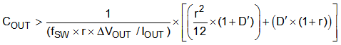
where
- r = Ripple ratio of the inductor ripple current (ILripple / 6 A )
- ΔVOUT = Target output voltage undershoot, for example, 5% to 10% of VOUT
- D’ = 1 – duty cycle
- fSW = switching frequency
- IOUT = load current
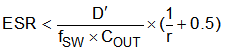
Along with Equation 28, for the same requirement calculate the maximum ESR with Equation 29.
The output capacitor is also the dominating factor in the loop response of a peak-current mode controlled buck converter. A simplified estimation of the control loop crossover frequency can be found by Equation 18.
Select COUT so that the fX is no higher than 1/6 of the switching frequency. Typically, fX / fSW = 1/10 to 1/8 provides a good combination of stability and performance.
For this design, one 0.47-µF, 50-V X7R and four 22-µF, 16-V, X7R ceramic capacitors are used in parallel based on a target output voltage overshoot value of 10%.