SNVSBL0A November 2020 – December 2021 TPS7H4010-SEP
PRODUCTION DATA
- 1 Features
- 2 Applications
- 3 Description
- 4 Revision History
- 5 Pin Configuration and Functions
- 6 Specifications
-
7 Detailed Description
- 7.1 Overview
- 7.2 Functional Block Diagram
- 7.3
Feature Description
- 7.3.1 Synchronous Step-Down Regulator
- 7.3.2 Auto Mode and FPWM Mode
- 7.3.3 Fixed-Frequency Peak Current-Mode Control
- 7.3.4 Adjustable Output Voltage
- 7.3.5 Enable and UVLO
- 7.3.6 Internal LDO, VCC_UVLO, and BIAS Input
- 7.3.7 Soft Start and Voltage Tracking
- 7.3.8 Adjustable Switching Frequency
- 7.3.9 Frequency Synchronization and Mode Setting
- 7.3.10 Internal Compensation and CFF
- 7.3.11 Bootstrap Capacitor and VBOOT-UVLO
- 7.3.12 Power-Good and Overvoltage Protection
- 7.3.13 Overcurrent and Short-Circuit Protection
- 7.3.14 Thermal Shutdown
- 7.4 Device Functional Modes
-
8 Application and Implementation
- 8.1 Application Information
- 8.2
Typical Application
- 8.2.1 Design Requirements
- 8.2.2
Detailed Design Procedure
- 8.2.2.1 Output Voltage Setpoint
- 8.2.2.2 Switching Frequency
- 8.2.2.3 Input Capacitors
- 8.2.2.4 Inductor Selection
- 8.2.2.5 Output Capacitor Selection
- 8.2.2.6 Feed-Forward Capacitor
- 8.2.2.7 Bootstrap Capacitors
- 8.2.2.8 VCC Capacitor
- 8.2.2.9 BIAS
- 8.2.2.10 Soft Start
- 8.2.2.11 Undervoltage Lockout Setpoint
- 8.2.2.12 PGOOD
- 8.2.3 Application Curves
- 9 Power Supply Recommendations
- 10Layout
- 11Device and Documentation Support
- 12Mechanical, Packaging, and Orderable Information
Package Options
Refer to the PDF data sheet for device specific package drawings
Mechanical Data (Package|Pins)
- RNP|30
- KGD|0
Thermal pad, mechanical data (Package|Pins)
- RNP|30
Orderable Information
7.3.2 Auto Mode and FPWM Mode
The TPS7H4010-SEP has pin configurable auto mode or FPWM options.
In auto mode, the device operates in diode emulation mode (DEM) at light loads. In DEM, inductor current stops flowing when it reaches 0 A. This is also referred to as discontinuous conduction mode (DCM). This is the same behavior as the non-synchronous regulator, with higher efficiency. At heavier load, when the inductor current valley is above 0 A, the device operates in continuous conduction mode (CCM), where the switching frequency is fixed and set by RT pin.
In auto mode, the peak inductor current has a minimum limit, IPEAK_MIN, in the TPS7H4010-SEP. When peak current reaches IPEAK_MIN, the switching frequency reduces to regulate the required load current. Switching frequency lowers when load reduces. This is when the device operates in pulse frequency modulation (PFM). PFM further improves efficiency by reducing switching losses. Light load efficiency is especially important for battery operated systems.
In forced PWM (FPWM) mode, the device operates in CCM regardless of load with the frequency set by RT pin or synchronization input. Inductor current can go negative at light loads. At light loads, the efficiency is lower than auto mode, due to higher conduction losses and switching losses. In FPWM, the device has fixed switching frequency over the entire load range, which is beneficial to noise sensitive applications.
Figure 7-2 shows the inductor current waveforms in each mode with heavy load, light load, and very light load. The difference between the two modes is at lighter loads where inductor current valley reaches zero.
 Figure 7-2 Inductor Current Waveforms at Auto Mode and
FPWM Mode With Different Loads
Figure 7-2 Inductor Current Waveforms at Auto Mode and
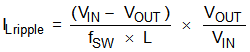
FPWM Mode With Different LoadsIn CCM, the inductor current peak-to-peak ripple can be estimated by Equation 1:
The average or DC value of the inductor current equals the load current, or output current IOUT, in steady state. Peak inductor current can be calculated by Equation 2:
Valley inductor current can be calculated by Equation 3:
In auto mode, the CCM to DCM boundary condition is when IVALLEY = 0 A. When ILripple ≥ IPEAK_MIN, the load current at the DCM boundary condition can be found by Equation 4. When the peak-to-peak ripple current is smaller than ILripple ≥ IPEAK-MIN, the PFM boundary will be reached first.
when
- ILripple ≥ IPEAK_MIN
In auto mode, the PFM operation boundary condition is when IPEAK = IPEAK_MIN. Frequency foldback occurs when peak current drops to IPEAK_MIN, no matter whether in CCM or DCM operation. When current ripple is small, ILripple < IPEAK_MIN, the peak current reaches IPEAK_MIN when still in CCM. The output current at CCM PFM boundary can be found by Equation 5:
when
- ILripple < IPEAK_MIN
The current ripple increases with reduced frequency if load reduces. When valley current reaches zero, the frequency continues to fold back with constant peak current and discontinuous current.
In FPWM mode, there is no IPEAK-MIN limit. The peak current is defined by Equation 2 at light loads and heavy loads.
Mode setting only affects operation at light loads. There is no difference if load current is above the DCM and PFM boundary conditions discussed above.
See Frequency Synchronization and Mode Setting section for mode setting options in TPS7H4010-SEP.