SNVSBL0A November 2020 – December 2021 TPS7H4010-SEP
PRODUCTION DATA
- 1 Features
- 2 Applications
- 3 Description
- 4 Revision History
- 5 Pin Configuration and Functions
- 6 Specifications
-
7 Detailed Description
- 7.1 Overview
- 7.2 Functional Block Diagram
- 7.3
Feature Description
- 7.3.1 Synchronous Step-Down Regulator
- 7.3.2 Auto Mode and FPWM Mode
- 7.3.3 Fixed-Frequency Peak Current-Mode Control
- 7.3.4 Adjustable Output Voltage
- 7.3.5 Enable and UVLO
- 7.3.6 Internal LDO, VCC_UVLO, and BIAS Input
- 7.3.7 Soft Start and Voltage Tracking
- 7.3.8 Adjustable Switching Frequency
- 7.3.9 Frequency Synchronization and Mode Setting
- 7.3.10 Internal Compensation and CFF
- 7.3.11 Bootstrap Capacitor and VBOOT-UVLO
- 7.3.12 Power-Good and Overvoltage Protection
- 7.3.13 Overcurrent and Short-Circuit Protection
- 7.3.14 Thermal Shutdown
- 7.4 Device Functional Modes
-
8 Application and Implementation
- 8.1 Application Information
- 8.2
Typical Application
- 8.2.1 Design Requirements
- 8.2.2
Detailed Design Procedure
- 8.2.2.1 Output Voltage Setpoint
- 8.2.2.2 Switching Frequency
- 8.2.2.3 Input Capacitors
- 8.2.2.4 Inductor Selection
- 8.2.2.5 Output Capacitor Selection
- 8.2.2.6 Feed-Forward Capacitor
- 8.2.2.7 Bootstrap Capacitors
- 8.2.2.8 VCC Capacitor
- 8.2.2.9 BIAS
- 8.2.2.10 Soft Start
- 8.2.2.11 Undervoltage Lockout Setpoint
- 8.2.2.12 PGOOD
- 8.2.3 Application Curves
- 9 Power Supply Recommendations
- 10Layout
- 11Device and Documentation Support
- 12Mechanical, Packaging, and Orderable Information
Package Options
Refer to the PDF data sheet for device specific package drawings
Mechanical Data (Package|Pins)
- RNP|30
- KGD|0
Thermal pad, mechanical data (Package|Pins)
- RNP|30
Orderable Information
7.3.10 Internal Compensation and CFF
The TPS7H4010-SEP is internally compensated. The internal compensation is designed such that the loop response is stable over a wide operating frequency and output voltage range. The internal R-C values are 500 kΩ and 30 pF, respectively.
When large resistance value (MΩ) is used for RFBT, the pole formed by an internal parasitic capacitor and RFBT can be low enough to reduce the phase margin. If only low ESR output capacitors (ceramic types) are used for COUT, the control loop could have low phase margin. To provide a phase boost an external feed-forward capacitor (CFF) can be added in parallel with RFBT. Choose the CFF capacitor to provide most phase boost at the estimated crossover frequency fX:
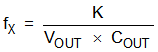
where
- K = 24.16 with TPS7H4010-SEP
Select COUT so that the fX is no higher than 1/6 of the switching frequency. Typically, fX / fSW = 1/10 to 1/8 provides a good combination of stability and performance.
Place the external feed-forward capacitor in parallel with the top resistor divider RFBT when additional phase boost is needed.
 Figure 7-14 Feed-Forward Capacitor for Loop Compensation
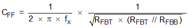
The feed-forward capacitor CFF in parallel with RFBT places an additional zero before the crossover frequency of the control loop to boost phase margin. The zero frequency can be found by Equation 19:
An additional pole is also introduced with CFF at the frequency of:
Select the CFF so that the bandwidth of the control loop without the CFF is centered between fZ-CFF and fP-CFF. The zero at fZ-CFF adds phase boost at the crossover frequency and improves transient response. The pole at fP-CFF helps maintaining proper gain margin at frequency beyond the crossover.
The need of CFF depends on RFBT and COUT. Typically, choose RFBT ≤ 100 kΩ. CFF may not be required, because the internal parasitic pole is at higher frequency. If COUT has larger ESR, and ESR zero fZ-ESR = 1 / (2π × ESR × COUT) is low enough to provide phase boost around the crossover frequency, do not use CFF. Equation 21 was tested for ceramic output capacitors:
The CFF creates a time constant with RFBT that couples in the attenuated output voltage ripple to the FB node. If the CFF value is too large, it can couple too much ripple to the FB and affect VOUT regulation. It could also couple too much transient voltage deviation and falsely trigger PGOOD flag.