SLVSAZ9D June 2012 – February 2018 TPS81256
PRODUCTION DATA.
- 1 Features
- 2 Applications
- 3 Description
- 4 Revision History
- 5 Device Options
- 6 Pin Configuration and Functions
- 7 Specifications
- 8 Detailed Description
- 9 Application and Implementation
- 10Power Supply Recommendations
- 11Layout
- 12Device and Documentation Support
- 13Mechanical, Packaging, and Orderable Information
Package Options
Refer to the PDF data sheet for device specific package drawings
Mechanical Data (Package|Pins)
- SIP|9
Thermal pad, mechanical data (Package|Pins)
Orderable Information
11.4 Thermal and Reliability Information
The TPS81256 output current may need to be de-rated if it is required to operate in a high ambient temperature or deliver a large amount of continuous power. The amount of current de-rating is dependent upon the input voltage, output power and environmental thermal conditions. Care should especially be taken in applications where the localized PWB temperature exceeds 65°C.
The TPS81256 die and inductor temperature should be kept lower than the maximum rating of 125°C, so care should be taken in the circuit layout to ensure good heat sinking. Sufficient cooling should be provided to ensure reliable operation.
To estimate the junction temperature, approximate the power dissipation within the TPS81256 by applying the typical efficiency stated in this datasheet to the desired output power; or, by taking a power measurement if you have an actual TPS81256 device or a TPS81256EVM evaluation module. Then calculate the internal temperature rise of the TPS81256 above the surface of the printed circuit board by multiplying the TPS81256 power dissipation by the thermal resistance.
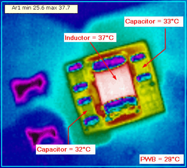
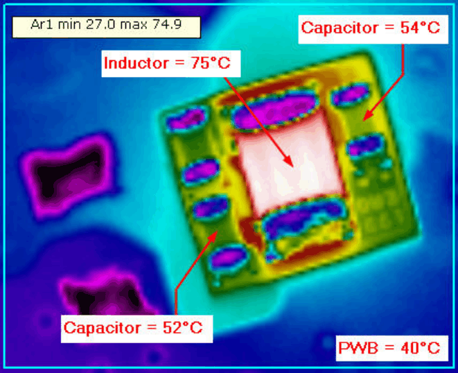
The thermal resistance numbers listed in the Thermal Information table are based on modeling the MicroSiP package mounted on a high-K test board specified per JEDEC standard. For increased accuracy and fidelity to the actual application, it is recommended to run a thermal image analysis of the actual system. Figure 24 and Figure 25 are thermal images of TI’s evaluation board with readings of the temperatures at specific locations on the device.
 Figure 24. VIN=3.6v, VOUT=5v, IOUT=300ma
150mw Power Dissipation At Room Temperature
 Figure 25. VIN=3.6v, VOUT=5v, IOUT=600ma
600mw Power Dissipation At Room Temperature
The TPS81256 is equipped with a thermal shutdown that will inhibit power switching at high junction temperatures. The activation threshold of this function, however, is above 125°C to avoid interfering with normal operation. Thus, it follows that prolonged or repetitive operation under a condition in which the thermal shutdown activates necessarily means that the components internal to the MicroSiP™ package are subjected to high temperatures for prolonged or repetitive intervals, which may damage or impair the reliability of the device.
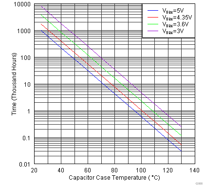
MLCC capacitor reliability/lifetime is dependant on temperature and applied voltage conditions. At higher temperatures, MLCC capacitors are subject to stronger stress. On the basis of frequently evaluated failure rates determined at standardized test conditions, the reliability of all MLCC capacitors can be calculated for their actual operating temperature and voltage.
 Figure 26. Capacitor Lifetime vs Capacitor Case Temperature
Failures caused by systematic degradation can be described by the Arrhenius model. The most critical parameter (IR) is the Insulation Resistance (i.e. leakage current). The drop of IR below a lower limit (e.g. 1 MΩ) is used as the failure criterion, see Figure 26. It should be noted that the wear-out mechanisms occurring in the MLCC capacitors are not reversible but cumulative over time.