SLVSDN4 June   2017 TPS82150

PRODUCTION DATA.  

  1. Features
  2. Applications
  3. Description
    1.     Device Images
      1.      Typical Application Schematic spacespace
      2.      Efficiency vs Output Current, VIN=12V space
  4. Revision History
  5. Pin Configuration and Functions
    1.     Pin Functions
  6. Specifications
    1. 6.1 Absolute Maximum Ratings
    2. 6.2 ESD Ratings
    3. 6.3 Recommend Operating Conditions
    4. 6.4 Thermal Information
    5. 6.5 Electrical Characteristics
    6. 6.6 Typical Characteristics
  7. Detailed Description
    1. 7.1 Overview
    2. 7.2 Functional Block Diagram
    3. 7.3 Feature Description
      1. 7.3.1 PWM and PSM Operation
      2. 7.3.2 Low Dropout Operation (100% Duty Cycle)
      3. 7.3.3 Switch Current Limit
      4. 7.3.4 Undervoltage Lockout
      5. 7.3.5 Thermal Shutdown
    4. 7.4 Device Functional Modes
      1. 7.4.1 Enable and Disable (EN)
      2. 7.4.2 Soft Startup (SS/TR)
      3. 7.4.3 Voltage Tracking (SS/TR)
      4. 7.4.4 Power Good Output (PG)
  8. Application and Implementation
    1. 8.1 Application Information
    2. 8.2 Typical Applications
      1. 8.2.1 1.8-V Output Application
        1. 8.2.1.1 Design Requirements
        2. 8.2.1.2 Detailed Design Procedure
          1. 8.2.1.2.1 Custom Design with WEBENCH® Tools
          2. 8.2.1.2.2 Setting the Output Voltage
          3. 8.2.1.2.3 Input and Output Capacitor Selection
          4. 8.2.1.2.4 Soft Startup Capacitor Selection
        3. 8.2.1.3 Application Performance Curves
    3. 8.3 System Examples
      1. 8.3.1 Inverting Power Supply
  9. Power Supply Recommendations
  10. 10Layout
    1. 10.1 Layout Guidelines
    2. 10.2 Layout Example
    3. 10.3 Thermal Consideration
  11. 11Device and Documentation Support
    1. 11.1 Device Support
      1. 11.1.1 Third-Party Products Disclaimer
      2. 11.1.2 Development Support
        1. 11.1.2.1 Custom Design With WEBENCH® Tools
    2. 11.2 Receiving Notification of Documentation Updates
    3. 11.3 Community Resources
    4. 11.4 Trademarks
    5. 11.5 Electrostatic Discharge Caution
    6. 11.6 Glossary
  12. 12Mechanical, Packaging, and Orderable Information
    1. 12.1 Package Materials Information
      1. 12.1.1 Tape and Reel Information

Package Options

Mechanical Data (Package|Pins)
  • SIL|8
Thermal pad, mechanical data (Package|Pins)
Orderable Information

Inverting Power Supply

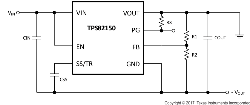
The TPS82150 can be used as inverting power supply by rearranging external circuitry as shown in Figure 30. As the former GND node now represents a voltage level below system ground, the voltage difference between VIN and VOUT has to be limited for operation to the maximum supply voltage of 17V (see Equation 8).

space

Equation 8. TPS82150 SLVSDN4_eqinv.gif

space

space

TPS82150 SLVSDN4_inverter.gifFigure 30. Inverting Power Supply Schematic

space

The transfer function of the inverting power supply configuration differs from the buck mode transfer function, incorporating a Right Half Plane Zero additionally. Therefore the loop stability has to be adapted. More detailed information is given in TIDUCV2.