SLUSEG1A August 2021 – December 2021 TPS92519-Q1
PRODUCTION DATA
- 1 Features
- 2 Applications
- 3 Description
- 4 Revision History
- 5 Pin Configuration and Functions
- 6 Specifications
-
7 Detailed Description
- 7.1 Overview
- 7.2 Functional Block Diagram
- 7.3
Feature Description
- 7.3.1 Buck Converter Switching Operation
- 7.3.2 Switching Frequency and Adaptive On-Time Control
- 7.3.3 Minimum On-Time, Off-Time, and Inductor Ripple
- 7.3.4 Enable
- 7.3.5 LED Current Regulation and Error Amplifier
- 7.3.6 Start-up Sequence
- 7.3.7 Analog Dimming and Forced Continuous Conduction Mode
- 7.3.8 External PWM Dimming and Input Undervoltage Lockout (UVLO)
- 7.3.9 Shunt FET Dimming or Matrix Beam Application
- 7.3.10 Bias Supply
- 7.3.11 Bootstrap Supply
- 7.3.12 Faults and Diagnostics
- 7.3.13 Output Short Circuit Fault
- 7.3.14 Output Open Circuit Fault
- 7.3.15 Parallel Operation
- 7.4 Device Functional Modes
-
8 Application and Implementation
- 8.1
Application Information
- 8.1.1 Duty Cycle Consideration
- 8.1.2 Switching Frequency Selection
- 8.1.3 LED Current Set Point
- 8.1.4 Inductor Selection
- 8.1.5 Output Capacitor Selection
- 8.1.6 Input Capacitor Selection
- 8.1.7 Bootstrap Capacitor Selection
- 8.1.8 Compensation Capacitor Selection
- 8.1.9 Input Undervoltage Protection
- 8.1.10 CSN Protection Diode
- 8.2
Typical Application
- 8.2.1 Design Requirements
- 8.2.2
Detailed Design Procedure
- 8.2.2.1 Calculating Duty Cycle
- 8.2.2.2 Calculating Minimum On-Time and Off-Time
- 8.2.2.3 Minimum Switching Frequency
- 8.2.2.4 LED Current Set Point
- 8.2.2.5 Inductor Selection
- 8.2.2.6 Output Capacitor Selection
- 8.2.2.7 Bootstrap Capacitor Selection
- 8.2.2.8 Compensation Capacitor Selection
- 8.2.2.9 PWM Dimming and Input Voltage Protection
- 8.2.3 Application Curves
- 8.1
Application Information
- 9 Power Supply Recommendations
- 10Layout
- 11Device and Documentation Support
- 12Mechanical, Packaging, and Orderable Information
Package Options
Mechanical Data (Package|Pins)
- DAP|32
Thermal pad, mechanical data (Package|Pins)
- DAP|32
Orderable Information
7.3.15 Parallel Operation
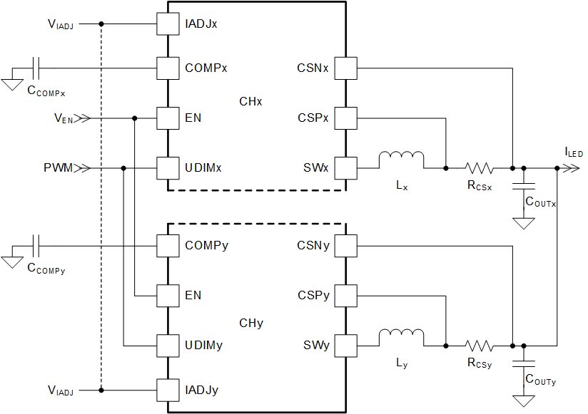
The adaptive on-time control technique enables parallel operation of two or more channels with independent current sharing and regulation. Each channel operates independently and delivers current based on the corresponding IADJx set point. To equally share current amongst channels, the IADJx for all channels must be connected to the external reference voltage.
 Figure 7-11 Parallel Channel
Configuration
Figure 7-11 Parallel Channel
ConfigurationStartup requires all channels to be enabled simultaneously by synchronizing the rising edge of IADJx voltage above VIADJx(SD) rising threshold. This simultaneous enabling ensures that the soft-start ramp is synchronized and current sharing is achieved after COMP voltage increases above the rising startup threshold, VCOMPx(ST).
PWM dimming is achieved by connecting the external PWM signal to UDIMx pin of all parallel channels. All parallel channels have to be controlled by single PWM dimming reference. TI does not recommend to PWM dim individual parallel channels.
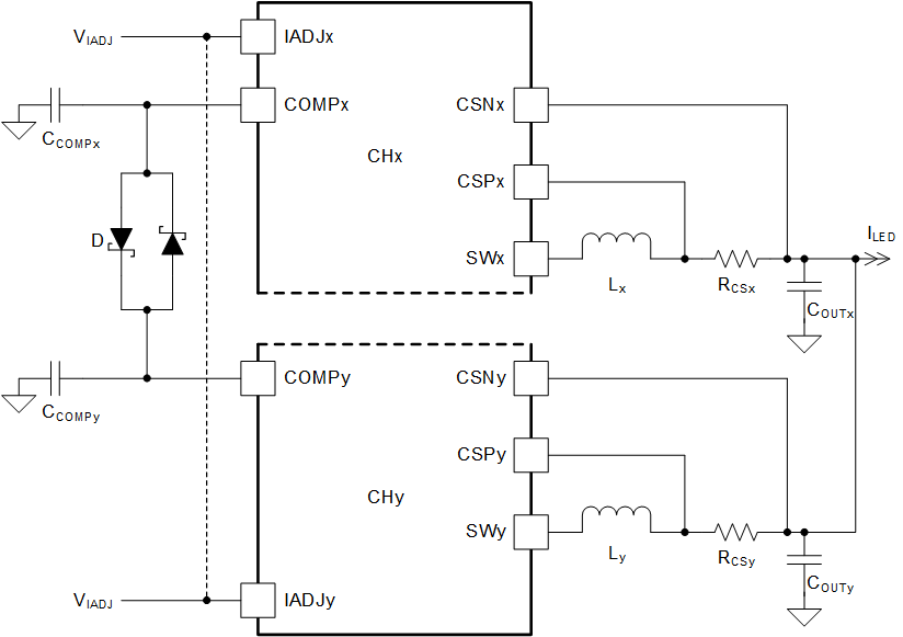
Additional considerations are necessary to account for bootstrap capacitor tolerance and the impact of the capacitor variation when PWM dimming multiple parallel channels. Ensure that bootstrap capacitor voltage is above the undervoltage threshold, VBSTx(UV) for all operating conditions. For application requiring very low PWM duty cycle or low PWM dimming frequency, TI recommends to connect the COMPx pin of all parallel channels using nonparallel diodes, as shown in Figure 7-12. This connection allows the parallel channels to respond and recovery from bootstrap undervoltage fault when operating at low PWM dimming duty cycles.
 Figure 7-12 Parallel Channel Configuration
for PWM Dimming Operation