SLUSEG1A August 2021 – December 2021 TPS92519-Q1
PRODUCTION DATA
- 1 Features
- 2 Applications
- 3 Description
- 4 Revision History
- 5 Pin Configuration and Functions
- 6 Specifications
-
7 Detailed Description
- 7.1 Overview
- 7.2 Functional Block Diagram
- 7.3
Feature Description
- 7.3.1 Buck Converter Switching Operation
- 7.3.2 Switching Frequency and Adaptive On-Time Control
- 7.3.3 Minimum On-Time, Off-Time, and Inductor Ripple
- 7.3.4 Enable
- 7.3.5 LED Current Regulation and Error Amplifier
- 7.3.6 Start-up Sequence
- 7.3.7 Analog Dimming and Forced Continuous Conduction Mode
- 7.3.8 External PWM Dimming and Input Undervoltage Lockout (UVLO)
- 7.3.9 Shunt FET Dimming or Matrix Beam Application
- 7.3.10 Bias Supply
- 7.3.11 Bootstrap Supply
- 7.3.12 Faults and Diagnostics
- 7.3.13 Output Short Circuit Fault
- 7.3.14 Output Open Circuit Fault
- 7.3.15 Parallel Operation
- 7.4 Device Functional Modes
-
8 Application and Implementation
- 8.1
Application Information
- 8.1.1 Duty Cycle Consideration
- 8.1.2 Switching Frequency Selection
- 8.1.3 LED Current Set Point
- 8.1.4 Inductor Selection
- 8.1.5 Output Capacitor Selection
- 8.1.6 Input Capacitor Selection
- 8.1.7 Bootstrap Capacitor Selection
- 8.1.8 Compensation Capacitor Selection
- 8.1.9 Input Undervoltage Protection
- 8.1.10 CSN Protection Diode
- 8.2
Typical Application
- 8.2.1 Design Requirements
- 8.2.2
Detailed Design Procedure
- 8.2.2.1 Calculating Duty Cycle
- 8.2.2.2 Calculating Minimum On-Time and Off-Time
- 8.2.2.3 Minimum Switching Frequency
- 8.2.2.4 LED Current Set Point
- 8.2.2.5 Inductor Selection
- 8.2.2.6 Output Capacitor Selection
- 8.2.2.7 Bootstrap Capacitor Selection
- 8.2.2.8 Compensation Capacitor Selection
- 8.2.2.9 PWM Dimming and Input Voltage Protection
- 8.2.3 Application Curves
- 8.1
Application Information
- 9 Power Supply Recommendations
- 10Layout
- 11Device and Documentation Support
- 12Mechanical, Packaging, and Orderable Information
Package Options
Mechanical Data (Package|Pins)
- DAP|32
Thermal pad, mechanical data (Package|Pins)
- DAP|32
Orderable Information
7.3.13 Output Short Circuit Fault
The TPS92519-Q1 monitors the CSNx voltage to detect output short circuit faults. A short failure is indicated when the CSNx voltage drops below 1.5 V. The corresponding is FLTx flag is set low. The device continues to regulate current and operate without interruption in case of short circuit.
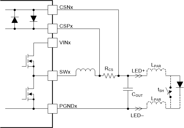
 Figure 7-6 Cable Harness Parasitic Inductance
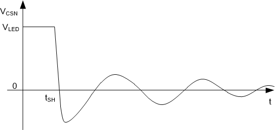
The voltage transient imposed on CSPx and CSNx inputs during short circuit is dependent on the output capacitance and is influenced by the cable harness impedance. The inductance associated with a long cable harness resonates with the charge stored on the output capacitor and forces CSPx and CSNx voltage to ring below ground. The negative voltage and current are dependent on the parasitic cable harness inductance and resistance.
 Figure 7-7 Short Circuit Fault Transient Behavior
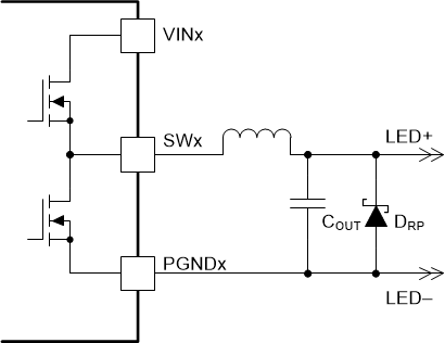
When using a long cable harness, TI recommends a diode to clamp the negative voltage across CSPx and CSNx input, as shown in Figure 7-8. TI recommends a low forward voltage Schottky diode or a fast recovery silicon diode with reverse blocking voltage rating greater than the maximum output voltage. The diode is required to be placed close to the output capacitor and must ensure that the current flowing through CSP and CSN nodes under negative transient condition is below the absolute maximum rating of the device.
 Figure 7-8 CSP and CSN Transient Protection Using an External Diode