SLUSD66D September 2019 – February 2021 TPS92520-Q1
PRODUCTION DATA
- 1 Features
- 2 Applications
- 3 Description
- 4 Revision History
- 5 Pin Configuration and Functions
- 6 Specifications
-
7 Detailed Description
- 7.1 Overview
- 7.2 Functional Block Diagram
- 7.3
Feature Description
- 7.3.1 Buck Converter Switching Operation
- 7.3.2 Switching Frequency and Adaptive On-Time Control
- 7.3.3 Minimum On-Time, Off-Time, and Inductor Ripple
- 7.3.4 LED Current Regulation and Error Amplifier
- 7.3.5 Start-up Sequence
- 7.3.6 Analog Dimming and Forced Continuous Conduction Mode
- 7.3.7 External PWM Dimming and Input Undervoltage Lockout (UVLO)
- 7.3.8 Internal PWM Dimming
- 7.3.9 Shunt FET Dimming or Matrix Beam Application
- 7.3.10 Bias Supply
- 7.3.11 Bootstrap Supply
- 7.3.12 ADC
- 7.3.13 Faults and Diagnostics
- 7.3.14 Output Short Circuit Fault
- 7.3.15 Output Open Circuit Fault
- 7.4 Device Functional Modes
- 7.5 Programming
- 7.6
Register Maps
- 7.6.1 Configuration Registers
- 7.6.2 STATUS Registers
- 7.6.3
Device Control Registers
- 7.6.3.1 Thermal Warning Limit (address = 0x06) [reset = 0x8A]
- 7.6.3.2 SLEEP Command (address = 0x07) [reset = 0x00]
- 7.6.3.3 CH1IADJL Control Register (address = 0x08) [reset = 0x00]
- 7.6.3.4 CH1IADJH Control Register (address = 0x09) [reset = 0x00]
- 7.6.3.5 CH2IADJL Control Register (address = 0x0A) [reset = 0x00]
- 7.6.3.6 CH2IADJH Control Register (address = 0x0B) [reset = 0x00]
- 7.6.3.7 PWMDIV Register (address = 0x0C) [reset = 0x04]
- 7.6.3.8 CH1PWML Register (address = 0x0D) [reset = 0x00]
- 7.6.3.9 CH1PWMH Register (address = 0x0E) [reset = 0x00]
- 7.6.3.10 CH2PWML Register (address = 0x0F) [reset = 0x00]
- 7.6.3.11 CH2PWMH Register (address = 0x10) [reset = 0x00]
- 7.6.3.12 CH1TON Register (address = 0x11) [reset = 0x07]
- 7.6.3.13 CH2TON Register (address = 0x12) [reset = 0x07]
- 7.6.4
ADC Measurements
- 7.6.4.1 CH1VIN Measurement (address = 0x13)
- 7.6.4.2 CH1VLED Measurement (address = 0x14)
- 7.6.4.3 CH1VLEDON Measurement (address = 0x15)
- 7.6.4.4 CH1VLEDOFF Measurement (address = 0x16)
- 7.6.4.5 CH2VIN Measurement (address = 0x17)
- 7.6.4.6 CH2VLED Measurement (address = 0x18)
- 7.6.4.7 CH2VLEDON Measurement (address = 0x19)
- 7.6.4.8 CH2VLEDOFF Measurement (address = 0x1A)
- 7.6.4.9 TEMPL Measurement (address = 0x1B)
- 7.6.4.10 TEMPH Measurement (address = 0x1C)
- 7.6.4.11 V5D Measurement (address = 0x1D)
- 7.6.5
Limp-Home Configuration and Command Registers
- 7.6.5.1 LHCFG1 Register (address = 0x1E) [reset =0x00]
- 7.6.5.2 LHCFG2 Register (address = 0x1F) [reset =0x00h]
- 7.6.5.3 LHIL Measurement (address = 0x20)
- 7.6.5.4 LHIH Measurement (address = 0x21)
- 7.6.5.5 LHIFILTL Register (address = 0x22)
- 7.6.5.6 LHIFILTH Register (address = 0x23)
- 7.6.5.7 LH1IADJL Register (address = 0x24) [reset = 0x00]
- 7.6.5.8 LH1IADJH Register (address = 0x25) [reset = 0x00]
- 7.6.5.9 LH2IADJL Register (address = 0x26) [reset = 0x00]
- 7.6.5.10 LH2IADJH Register (address = 0x27) [reset = 0x00]
- 7.6.5.11 LH1PWML Register (address = 0x28) [reset = 0x00]
- 7.6.5.12 LH1PWMH Register (address = 0x29) [reset = 0x00]
- 7.6.5.13 LH2PWML Register (address = 0x2A) [reset = 0x00]
- 7.6.5.14 LH2PWMH Register (address = 0x2B) [reset = 0x00]
- 7.6.5.15 LH1TON Register (address = 0x2C) [reset = 0x07]
- 7.6.5.16 LH2TON Register (address = 0x2D) [reset = 0x07]
- 7.6.6 RESET Register (address = 0x2E) (Write-Only)
-
8 Application and Implementation
- 8.1
Application Information
- 8.1.1 Duty Cycle Consideration
- 8.1.2 Switching Frequency Selection
- 8.1.3 LED Current Set Point
- 8.1.4 Inductor Selection
- 8.1.5 Output Capacitor Selection
- 8.1.6 Input Capacitor Selection
- 8.1.7 Bootstrap Capacitor Selection
- 8.1.8 Compensation Capacitor Selection
- 8.1.9 Input Undervoltage Protection
- 8.1.10 CSN Protection Diode
- 8.2
Typical Application
- 8.2.1
Design Requirements
- 8.2.1.1
Detailed Design Procedure
- 8.2.1.1.1 Calculating Duty Cycle
- 8.2.1.1.2 Calculating Minimum On-Time and Off-Time
- 8.2.1.1.3 Minimum Switching Frequency
- 8.2.1.1.4 LED Current Set Point
- 8.2.1.1.5 Inductor Selection
- 8.2.1.1.6 Output Capacitor Selection
- 8.2.1.1.7 Bootstrap Capacitor Selection
- 8.2.1.1.8 Compensation Capacitor Selection
- 8.2.1.1.9 External Channel Enable and PWM dimming
- 8.2.1.1
Detailed Design Procedure
- 8.2.2 Application Curves
- 8.2.1
Design Requirements
- 8.3 Initialization Setup
- 8.1
Application Information
- 9 Power Supply Recommendations
- 10Layout
- 11Device and Documentation Support
- 12Mechanical, Packaging, and Orderable Information
Package Options
Mechanical Data (Package|Pins)
Thermal pad, mechanical data (Package|Pins)
Orderable Information
7.3.15 Output Open Circuit Fault
An LED open circuit fault ultimately causes the output voltage to increase and settle close to the input voltage. When this occurs, the TPS92520-Q1 switching operation is then controlled by the fixed on-time and minimum off-time resulting in a duty cycle close to 100%. However during open circuit, the dynamic behavior of the device and buck converter is influenced by the input voltage, VIN, and the output capacitor, COUT, value. The device response to open circuit can be categorized into the following three distinct cases.
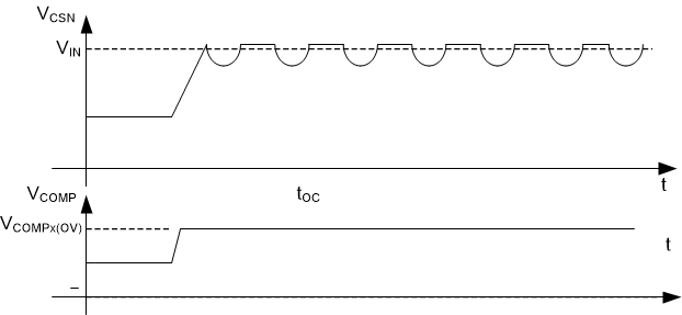
Case 1: For a Buck converter design with a small output capacitor, the switching operation in open load condition excites the inductor and the output capacitor resonance, forcing the output voltage to oscillate. The frequency and amplitude of the oscillation are based on the resonant frequency and Q-factor of the tank. The open-circuit is detected by checking the CHxCOMPOV, CHxTOFFMIN bits in STATUS1 and STATUS2 registers and by polling the CHxVLED register to verify the output voltage measured by internal ADC.
 Figure 7-10 Open Circuit Condition with Output Voltage Oscillation
Case 2: For a buck converter design with larger output capacitor, the inductor Q-factor and resonant frequency are much lower than the switching frequency. In this case, output voltage rises to input voltage and the converter continues to switch with minimum off-time. The open-circuit fault is detected by checking the CHxTOFFMIN bit in STATUS2 register and by polling the CHxVLED register to verify the output voltage measured by internal ADC.
 Figure 7-11 Open circuit Condition with Minimum Off-time Operation
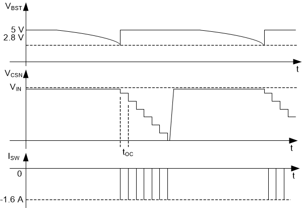
Case 3: When operating at higher input voltage, the larger gate-to-drain charge depletes the bootstrap capacitor and triggers bootstrap UVLO protection. When bootstrap voltage is below 2.95 V, undervoltage protection is triggered. Due to insufficient gate drive supply, the high-side MOSFET RDSON is larger than typical value tripping the high side current limit circuit. On detection of high-side current limit, the low-side FET is turned on, causing the output capacitor to discharge and trip the low-side current limit. Further attempts to restart the converter cause the low-side protection to trigger and the sequence continues until the output capacitor is discharged to ground. The operation is illustrated in Figure 7-12.
 Figure 7-12 Open Circuit Condition with Bootstrap Undervoltage Lockout Fault
The open circuit can be detected by reading the CHxHSILIM, CHxLSILIM bits in the STATUS1 register and CHxBSTUV bit in the STATUS2 register in conjunction with the CHxTOFFMIN and CHxVLED register. The microcontroller can detect and respond to open circuit by polling CHxVLED register in conjunction with reading CHxTOFFMIN, CHxLSILIM, and CHxBSTUV bits.
Table 7-3 summarizes the device response to open circuit faults. The device can transition between different modes near the input voltage range of 40 V to 50 V. TI recommends polling STATUS1, STATUS2, and STATUS3 registers to correctly identify an open circuit fault based on the specified input voltage range and choice of output capacitor.
| VCSNx ADC | CHxCOMPOV | CHxTOFFMIN | CHxBSTUV | CHxHSILIM | CHxLSILIM | CHxSHORT | |
|---|---|---|---|---|---|---|---|
| Case 1 | Read CSNx ADC measurement | 1 | 1 | 0 | 0 | 0 | 0 |
| Case 2 | Read CSNx ADC measurement | 0 | 1 | 0 | 0 | 0 | 0 |
| Case 3 | Ignore CSNx ADC measurement | x | x | 1 | 1 | 1 | 1 |