SLUSD66D September 2019 – February 2021 TPS92520-Q1
PRODUCTION DATA
- 1 Features
- 2 Applications
- 3 Description
- 4 Revision History
- 5 Pin Configuration and Functions
- 6 Specifications
-
7 Detailed Description
- 7.1 Overview
- 7.2 Functional Block Diagram
- 7.3
Feature Description
- 7.3.1 Buck Converter Switching Operation
- 7.3.2 Switching Frequency and Adaptive On-Time Control
- 7.3.3 Minimum On-Time, Off-Time, and Inductor Ripple
- 7.3.4 LED Current Regulation and Error Amplifier
- 7.3.5 Start-up Sequence
- 7.3.6 Analog Dimming and Forced Continuous Conduction Mode
- 7.3.7 External PWM Dimming and Input Undervoltage Lockout (UVLO)
- 7.3.8 Internal PWM Dimming
- 7.3.9 Shunt FET Dimming or Matrix Beam Application
- 7.3.10 Bias Supply
- 7.3.11 Bootstrap Supply
- 7.3.12 ADC
- 7.3.13 Faults and Diagnostics
- 7.3.14 Output Short Circuit Fault
- 7.3.15 Output Open Circuit Fault
- 7.4 Device Functional Modes
- 7.5 Programming
- 7.6
Register Maps
- 7.6.1 Configuration Registers
- 7.6.2 STATUS Registers
- 7.6.3
Device Control Registers
- 7.6.3.1 Thermal Warning Limit (address = 0x06) [reset = 0x8A]
- 7.6.3.2 SLEEP Command (address = 0x07) [reset = 0x00]
- 7.6.3.3 CH1IADJL Control Register (address = 0x08) [reset = 0x00]
- 7.6.3.4 CH1IADJH Control Register (address = 0x09) [reset = 0x00]
- 7.6.3.5 CH2IADJL Control Register (address = 0x0A) [reset = 0x00]
- 7.6.3.6 CH2IADJH Control Register (address = 0x0B) [reset = 0x00]
- 7.6.3.7 PWMDIV Register (address = 0x0C) [reset = 0x04]
- 7.6.3.8 CH1PWML Register (address = 0x0D) [reset = 0x00]
- 7.6.3.9 CH1PWMH Register (address = 0x0E) [reset = 0x00]
- 7.6.3.10 CH2PWML Register (address = 0x0F) [reset = 0x00]
- 7.6.3.11 CH2PWMH Register (address = 0x10) [reset = 0x00]
- 7.6.3.12 CH1TON Register (address = 0x11) [reset = 0x07]
- 7.6.3.13 CH2TON Register (address = 0x12) [reset = 0x07]
- 7.6.4
ADC Measurements
- 7.6.4.1 CH1VIN Measurement (address = 0x13)
- 7.6.4.2 CH1VLED Measurement (address = 0x14)
- 7.6.4.3 CH1VLEDON Measurement (address = 0x15)
- 7.6.4.4 CH1VLEDOFF Measurement (address = 0x16)
- 7.6.4.5 CH2VIN Measurement (address = 0x17)
- 7.6.4.6 CH2VLED Measurement (address = 0x18)
- 7.6.4.7 CH2VLEDON Measurement (address = 0x19)
- 7.6.4.8 CH2VLEDOFF Measurement (address = 0x1A)
- 7.6.4.9 TEMPL Measurement (address = 0x1B)
- 7.6.4.10 TEMPH Measurement (address = 0x1C)
- 7.6.4.11 V5D Measurement (address = 0x1D)
- 7.6.5
Limp-Home Configuration and Command Registers
- 7.6.5.1 LHCFG1 Register (address = 0x1E) [reset =0x00]
- 7.6.5.2 LHCFG2 Register (address = 0x1F) [reset =0x00h]
- 7.6.5.3 LHIL Measurement (address = 0x20)
- 7.6.5.4 LHIH Measurement (address = 0x21)
- 7.6.5.5 LHIFILTL Register (address = 0x22)
- 7.6.5.6 LHIFILTH Register (address = 0x23)
- 7.6.5.7 LH1IADJL Register (address = 0x24) [reset = 0x00]
- 7.6.5.8 LH1IADJH Register (address = 0x25) [reset = 0x00]
- 7.6.5.9 LH2IADJL Register (address = 0x26) [reset = 0x00]
- 7.6.5.10 LH2IADJH Register (address = 0x27) [reset = 0x00]
- 7.6.5.11 LH1PWML Register (address = 0x28) [reset = 0x00]
- 7.6.5.12 LH1PWMH Register (address = 0x29) [reset = 0x00]
- 7.6.5.13 LH2PWML Register (address = 0x2A) [reset = 0x00]
- 7.6.5.14 LH2PWMH Register (address = 0x2B) [reset = 0x00]
- 7.6.5.15 LH1TON Register (address = 0x2C) [reset = 0x07]
- 7.6.5.16 LH2TON Register (address = 0x2D) [reset = 0x07]
- 7.6.6 RESET Register (address = 0x2E) (Write-Only)
-
8 Application and Implementation
- 8.1
Application Information
- 8.1.1 Duty Cycle Consideration
- 8.1.2 Switching Frequency Selection
- 8.1.3 LED Current Set Point
- 8.1.4 Inductor Selection
- 8.1.5 Output Capacitor Selection
- 8.1.6 Input Capacitor Selection
- 8.1.7 Bootstrap Capacitor Selection
- 8.1.8 Compensation Capacitor Selection
- 8.1.9 Input Undervoltage Protection
- 8.1.10 CSN Protection Diode
- 8.2
Typical Application
- 8.2.1
Design Requirements
- 8.2.1.1
Detailed Design Procedure
- 8.2.1.1.1 Calculating Duty Cycle
- 8.2.1.1.2 Calculating Minimum On-Time and Off-Time
- 8.2.1.1.3 Minimum Switching Frequency
- 8.2.1.1.4 LED Current Set Point
- 8.2.1.1.5 Inductor Selection
- 8.2.1.1.6 Output Capacitor Selection
- 8.2.1.1.7 Bootstrap Capacitor Selection
- 8.2.1.1.8 Compensation Capacitor Selection
- 8.2.1.1.9 External Channel Enable and PWM dimming
- 8.2.1.1
Detailed Design Procedure
- 8.2.2 Application Curves
- 8.2.1
Design Requirements
- 8.3 Initialization Setup
- 8.1
Application Information
- 9 Power Supply Recommendations
- 10Layout
- 11Device and Documentation Support
- 12Mechanical, Packaging, and Orderable Information
Package Options
Mechanical Data (Package|Pins)
Thermal pad, mechanical data (Package|Pins)
Orderable Information
7.4.7 Limp-Home Mode
The TPS92520-Q1 enters the limp-home mode after detecting three consecutive watchdog timeout events or when the LHSW bit is set high in the SYSCFG1 register. In limp-home mode, the device sets the operation based on the SPI-programmable LH-registers (register address 0x1E to 0x2D). The limp-home registers must be programmed upon the initialization of the device in load mode.
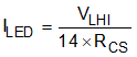
The LED current reference can be programmed through the LHxIADJ registers or set by external voltage measured at the LHI pin by the ADC. To enable LED control by the LHI pin, set the LHEXTIADJ bit in the LHCFG1 register to "1". Equation 14 expresses the relationship between the LED current and voltage at the LHI pin, VLHI.
The LHI voltage measured by the ADC is converted to a 10-bit value and stored in the LHI registers. An internal digital low pass filter attenuates any switching noise coupled to the LHI pin. The output of the filter is stored in the LHIFILT registers.
When the external LHI pin is selected as the LED current reference, an LHI pin voltage below 148 mV disables both channels and turns off the LEDs. In this condition, the device ensures that no light output is generated for the associated channels. The LHI pin voltage has to exceed 200 mV to enable both channels. The hysteresis rejects external noise on LHI pin and avoids light flickering.
To exit limp-home mode, the contents of STATUS3 register must be read to clear the CMWTO bits followed by a write command to set the LHSW bit in the SYSCFG1 register to "0".