SLVSEC4B April   2019  – January 2020 TPS92613-Q1

PRODUCTION DATA.  

  1. Features
  2. Applications
  3. Description
    1.     Device Images
      1.      Typical Application Diagram
  4. Revision History
  5. Pin Configuration and Functions
    1.     Pin Functions
  6. Specifications
    1. 6.1 Absolute Maximum Ratings
    2. 6.2 ESD Ratings
    3. 6.3 Recommended Operating Conditions
    4. 6.4 Thermal Information
    5. 6.5 Electrical Characteristics
    6. 6.6 Timing Requirements
    7. 6.7 Typical Characteristics
  7. Detailed Description
    1. 7.1 Overview
    2. 7.2 Functional Block Diagram
    3. 7.3 Feature Description
      1. 7.3.1 Power Supply
        1. 7.3.1.1 Power-On Reset (POR)
        2. 7.3.1.2 Low-Quiescent-Current
      2. 7.3.2 Constant-Current Driver
      3. 7.3.3 PWM Control
      4. 7.3.4 Supply Control
      5. 7.3.5 Diagnostics and Protection
        1. 7.3.5.1 Open-Circuit Detection
        2. 7.3.5.2 Short-to-GND Detection
        3. 7.3.5.3 Overtemperature Protection
        4. 7.3.5.4 DIAGEN
        5. 7.3.5.5 Low-Dropout Operation
      6. 7.3.6 FAULT Bus Output With One-Fails–All-Fail
      7. 7.3.7 Fault Table
    4. 7.4 Device Functional Modes
      1. 7.4.1 Undervoltage Lockout, V(SUPPLY) < V(POR_rising)
      2. 7.4.2 Normal Operation V(SUPPLY) ≥ 4.5 V
      3. 7.4.3 Low-Voltage Dropout Operation
      4. 7.4.4 Fault Mode
  8. Application and Implementation
    1. 8.1 Application Information
    2. 8.2 Typical Applications
      1. 8.2.1 Single-Channel LED Driver With Diagnostics
        1. 8.2.1.1 Design Requirements
        2. 8.2.1.2 Detailed Design Procedure
        3. 8.2.1.3 Application Curves
      2. 8.2.2 Single-Channel LED Driver With Heat Sharing
        1. 8.2.2.1 Design Requirements
        2. 8.2.2.2 Detailed Design Procedure
        3. 8.2.2.3 Application Curves
  9. Power Supply Recommendations
  10. 10Layout
    1. 10.1 Layout Guidelines
    2. 10.2 Layout Example
  11. 11Device and Documentation Support
    1. 11.1 Documentation Support
      1. 11.1.1 Related Documentation
    2. 11.2 Receiving Notification of Documentation Updates
    3. 11.3 Support Resources
    4. 11.4 Trademarks
    5. 11.5 Electrostatic Discharge Caution
    6. 11.6 Glossary
  12. 12Mechanical, Packaging, and Orderable Information

Package Options

Mechanical Data (Package|Pins)
Thermal pad, mechanical data (Package|Pins)
Orderable Information

Supply Control

The TPS92613-Q1 supports supply control to turn ON and OFF output current. When the voltage applied on the SUPPLY pin is higher than the LED string forward voltage plus needed V(DROPOUT) at required current, and the PWM pin voltage is high, the output current is turned ON and well regulated. However, if the voltage applied on the SUPPLY pin is lower than V(POR_falling), the output current is turned OFF. With this feature, the power-supply voltage in the designed pattern controls the output current ON/OFF. The brightness can be adjustable if the ON/OFF frequency is fast enough. Because of the high accuracy design of PWM threshold in TPS92613-Q1, TI recommends a resistor divider on the PWM pin to set the SUPPLY threshold higher than LED forward voltage plus V(DROPOUT) as shown in Figure 21. When the voltage on the PWM pin is higher than VIH(PWM), the output current is turned ON. However, when the voltage on the PWM is lower than VIL(PWM), the output current is turned OFF.
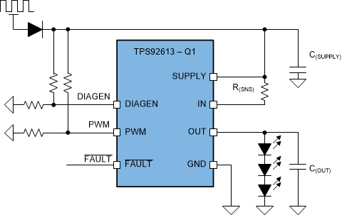
TPS92613-Q1 schem-05-slvsec4.gifFigure 21. Typical Application Schematic for SUPPLY Control