SLVSC76E February   2014  – May 2018 TPS92630-Q1

PRODUCTION DATA.  

  1. Features
  2. Applications
  3. Description
  4. Typical Application Schematic
  5. Revision History
  6. Description (Continued)
  7. Pin Configuration and Functions
    1.     Pin Functions
  8. Specifications
    1. 8.1 Absolute Maximum Ratings
    2. 8.2 ESD Ratings
    3. 8.3 Recommended Operating Conditions
    4. 8.4 Thermal Information
    5. 8.5 Electrical Characteristics
    6. 8.6 Timing Requirements
    7. 8.7 Typical Characteristics
  9. Parameter Measurement Information
  10. 10Detailed Description
    1. 10.1 Overview
    2. 10.2 Functional Block Diagram
    3. 10.3 Feature Description
      1. 10.3.1 Constant LED-Current Setting
      2. 10.3.2 PWM Control
      3. 10.3.3 FAULT Diagnostics
      4. 10.3.4 Short-Circuit Detection
      5. 10.3.5 Open-Load Detection
      6. 10.3.6 Thermal Foldback
    4. 10.4 Device Functional Modes
      1. 10.4.1 Thermal Information
      2. 10.4.2 Operation With V(VIN) < 5 V (Minimum V(VIN))
      3. 10.4.3 Operation With 5 V < V(VIN) < 9 V (Lower-Than-Normal Automotive Battery Voltage)
  11. 11Applications and Implementation
    1. 11.1 Application Information
    2. 11.2 Typical Applications
      1. 11.2.1 Stoplight and Taillight Application With PWM Generator
        1. 11.2.1.1 Design Requirements
        2. 11.2.1.2 Detailed Design Procedure
          1. 11.2.1.2.1 Step-by-Step Design Procedure
            1. 11.2.1.2.1.1 R(REF)
            2. 11.2.1.2.1.2 Duty Cycle
            3. 11.2.1.2.1.3 Input and Output Capacitors
        3. 11.2.1.3 PWM Dimming Application Curve
      2. 11.2.2 Simple Stop-Light and Taillight Application
        1. 11.2.2.1 Design Requirements
        2. 11.2.2.2 Detailed Design Procedure
          1. 11.2.2.2.1 Step-by-Step Design Procedure
            1. 11.2.2.2.1.1 R(REF)
            2. 11.2.2.2.1.2 R(Stop)
            3. 11.2.2.2.1.3 Input and Output Capacitors
      3. 11.2.3 Parallel Connection
        1. 11.2.3.1 Design Requirements
        2. 11.2.3.2 Detailed Design Procedure
          1. 11.2.3.2.1 Step-by-Step Design Procedure
            1. 11.2.3.2.1.1 R(REF)
            2. 11.2.3.2.1.2 Input and Output Capacitors
      4. 11.2.4 Alternate Parallel Connection
        1. 11.2.4.1 Design Requirements
        2. 11.2.4.2 Detailed Design Procedure
          1. 11.2.4.2.1 Step-by-Step Design Procedure
            1. 11.2.4.2.1.1 R(REF)
            2. 11.2.4.2.1.2 Input and Output Capacitors
      5. 11.2.5 High-Side PWM Dimming
        1. 11.2.5.1 Design Requirements
        2. 11.2.5.2 Detailed Design Procedure
          1. 11.2.5.2.1 Step-by-Step Design Procedure
            1. 11.2.5.2.1.1 Ratio of Resistors, R1 / R2
            2. 11.2.5.2.1.2 R1 and R2 Selection
            3. 11.2.5.2.1.3 Input and Output Capacitors
  12. 12Power Supply Recommendations
  13. 13Layout
    1. 13.1 Layout Guidelines
    2. 13.2 Layout Example
  14. 14Device and Documentation Support
    1. 14.1 Documentation Support
      1. 14.1.1 Related Documentation
    2. 14.2 Receiving Notification of Documentation Updates
    3. 14.3 Community Resources
    4. 14.4 Trademarks
    5. 14.5 Electrostatic Discharge Caution
    6. 14.6 Glossary
  15. 15Mechanical, Packaging, and Orderable Information

Package Options

Mechanical Data (Package|Pins)
Thermal pad, mechanical data (Package|Pins)
Orderable Information

Short-Circuit Detection

The device includes three internal comparators for LED forward-voltage measurement. With external resistor dividers, the device compares total LED forward voltage with the internal reference voltage. This feature enables the detection of one or more shorted LEDs. Any LED cathode or IOUTx pin shorted to ground results in a short-circuit condition. The external resistor dividers control the detection-threshold-voltage setting.

Figure 21 illustrates different short-circuit conditions.
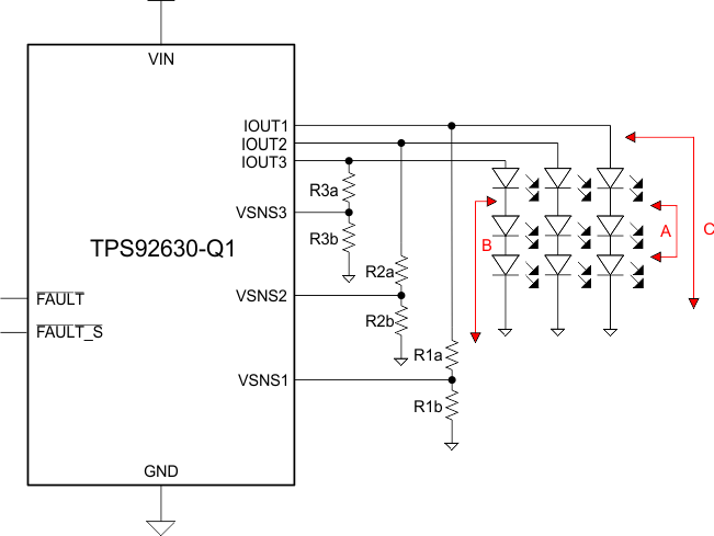
TPS92630-Q1 sho_cir_det_1_SLVSC76.gifFigure 21. Short-Circuit Conditions

A short in one or more LEDs in a string (A and B as illustrated) registers as only a single-LED short when V(VIN) > 9 V.

  • The device reports the failure to the MCU. The faulted channel continues sourcing current until the MCU takes actions to turn off channels through the EN or PWMx pin.
  • No MCU: with FAULT_S floating, no action results. With FAULT_S tied to FAULT, all output channels shut down together.

When an entire string of LEDs is shorted (C as illustrated), the device pulls FAULT low to shut down all channels. With the FAULT pin tied high, only the faulted channel turns off.

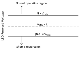
  • VF(max) – maximum forward voltage of LED used
  • VF(min) – minimum forward voltage of LED used
  • N – Number of LEDs used in a string
  • R – resistor divider ratio
  • V(VSNSx) – internal reference voltage of comparators

When selecting R, observe the following relationship to avoid false triggering.
Equation 2. R = (Rxa + Rxb) / Rxb
Equation 3. (N – 1) × VF(max)< V(VSNSx) × R < N × VF(min)
TPS92630-Q1 sho_cir_det_2_SLVSC76.gifFigure 22. Single-LED Short-Trigger Calculation