SLVSF65A December 2020 – May 2021 TPS92633-Q1
PRODUCTION DATA
- 1 Features
- 2 Applications
- 3 Description
- 4 Revision History
- 5 Pin Configuration and Functions
- 6 Specifications
-
7 Detailed Description
- 7.1 Overview
- 7.2 Functional Block Diagram
- 7.3
Feature Description
- 7.3.1 Power Supply (SUPPLY)
- 7.3.2 Enable and Shutdown (EN)
- 7.3.3 Reference Current (IREF)
- 7.3.4 Constant-Current Output and Setting (INx)
- 7.3.5 Analog Current Control (ICTRL)
- 7.3.6 Thermal Sharing Resistor (OUTx and RESx)
- 7.3.7 PWM Control (PWMx)
- 7.3.8 Supply Control
- 7.3.9
Diagnostics
- 7.3.9.1 IREF Short-to-GND Detection
- 7.3.9.2 IREF Open Detection
- 7.3.9.3 LED Short-to-GND Detection
- 7.3.9.4 LED Open-Circuit Detection
- 7.3.9.5 Single LED Short-Circuit Detection (SLS_REF)
- 7.3.9.6 LED Open-Circuit and Single LED Short-Circuit Detection Enable (DIAGEN)
- 7.3.9.7 Low Dropout Operation
- 7.3.9.8 Over-Temperature Protection
- 7.3.10 FAULT Bus Output With One-Fails–All-Fail
- 7.3.11 FAULT Table
- 7.3.12 LED Fault Summary
- 7.3.13 IO Pins Inner Connection
- 7.4 Device Functional Modes
- 8 Application and Implementation
- 9 Power Supply Recommendations
- 10Layout
- 11Device and Documentation Support
- 12Mechanical, Packaging, and Orderable Information
Package Options
Mechanical Data (Package|Pins)
- PWP|20
Thermal pad, mechanical data (Package|Pins)
- PWP|20
Orderable Information
8.2.2.2 Detailed Design Procedure
TI recommends to short the SLS_REF pin to GND when single-LED short-circuit is not required.
STEP 1: Determine the reference current setting resistor, R(IREF), by using Equation 15.
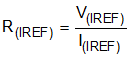
where
- V(IREF) = 1.235 V (typical)
- I(IREF) = 200 µA (recommended for off-board binning resistor)
TI recommends 200-µA current for reference current, I(IREF) if the ICTRL resistor is placed in the other board with TPS92633-Q1. The calculated result for R(IREF) is 6.19 kΩ when I(IREF) = 200 µA.
STEP 2: Design the ICTRL resistor, R(ICTRL1) and R(ICTRL2), for setting the regulation voltage, V(CS_REG), by using Equation 16.
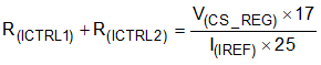
where
- I(IREF) = 200 µA (recommended for off-board binning resistor)
TI recommends 80 mV, 120 mV and 160 mV or reference voltage across current sensing resistor, R(SNSx), for three different brightness binning LED. The calculated result for R(ICTRL1) and R(ICTRL2) for different brightness bin LED is listed in Table 8-1. It is recommended to choose as large as possible R(ICTRL1) to achieve the highest noise immunity.
STEP 3: Determine the current sensing resistor, R(SNSx), by using Equation 17.
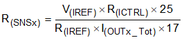
where
- V(IREF) = 1.235 V (typical)
- R(IREF) = 6.19 kΩ
According to design requirements, output current for each channel is same so that the R(SNS1) = R(SNS2) = R(SNS3). The calculated result for R(SNSx) is listed in Table 8-1.
| LED Brightness Group A | LED Brightness Group B | LED Brightness Group C | |
|---|---|---|---|
| I(OUTx_Tot) | 50 mA | 75 mA | 100 mA |
| V(CS_REG) | 80 mV | 120 mV | 160 mV |
| R(ICTRL1) + R(ICTRL2) | 272 Ω | 408 Ω | 544 Ω |
| R(ICTRL1) | 270 Ω | ||
| R(ICTRL2) | 2 Ω | 140 Ω | 274 Ω |
| R(SNSx) | 1.6 Ω | ||
STEP 4: Design the current distribution between I(OUTx) and I(RESx) and calculate the current sharing resistor, R(RESx), by using Equation 18. The R(RESx) value actually decides the current distribution for I(OUTx) path and I(RESx) path, basic principle is to design the R(RESx) to consume appropriate 50% total power dissipation at typical supply operating voltage.
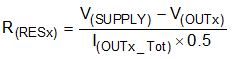
where
- V(SUPPLY) = 12 V (typical)
- I(OUTx_Tot) = 100 mA (maximum)
The calculated result for R(RESx) resistor value including R(RES1), R(RES2) and R(RES3) is 152 Ω when V(OUTx) is typical 2 × 2.2 V = 4.4 V.
STEP 5: Design the threshold voltage of SUPPLY to enable the LED open-circuit and single-LED short-circuit diagnostics, and calculate voltage divider resistor value for R1 and R2 on DIAGEN pin.
The maximum forward voltage of LED-string is 2 × 2.5 V = 5 V. To avoid the open-circuit fault reported in low-dropout operation conditions, additional headroom between SUPPLY and OUTx needs to be considered. The TPS92633-Q1 device must disable open-circuit detection when the supply voltage is below LED-string maximum forward voltage plus V(OPEN_th_rising) and V(CS_REG). The voltage divider resistor, R1 and R2 value can be calculated by Equation 19.
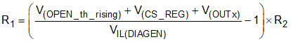
where
- V(OPEN_th_rising) = 210 mV (maximum)
- V(CS_REG) = 160 mV (maximum)
- VIL(DIAGEN) = 1.045 V (minimum)
- R2 = 10 kΩ (recommended)
The calculated result for R1 is 41.2 kΩ when V(OUTx) maximum voltage is 5 V and V(CS_REG) is 160 mV maximum.