SLVSFE8 June 2021 TPS92633
PRODUCTION DATA
- 1 Features
- 2 Applications
- 3 Description
- 4 Revision History
- 5 Pin Configuration and Functions
- 6 Specifications
-
7 Detailed Description
- 7.1 Overview
- 7.2 Functional Block Diagram
- 7.3
Feature Description
- 7.3.1 Power Supply (SUPPLY)
- 7.3.2 Enable and Shutdown (EN)
- 7.3.3 Reference Current (IREF)
- 7.3.4 Constant-Current Output and Setting (INx)
- 7.3.5 Analog Current Control (ICTRL)
- 7.3.6 Thermal Sharing Resistor (OUTx and RESx)
- 7.3.7 PWM Control (PWMx)
- 7.3.8 Supply Control
- 7.3.9
Diagnostics
- 7.3.9.1 IREF Short-to-GND Detection
- 7.3.9.2 IREF Open Detection
- 7.3.9.3 LED Short-to-GND Detection
- 7.3.9.4 LED Open-Circuit Detection
- 7.3.9.5 Single LED Short-Circuit Detection (SLS_REF)
- 7.3.9.6 LED Open-Circuit and Single LED Short-Circuit Detection Enable (DIAGEN)
- 7.3.9.7 Low Dropout Operation
- 7.3.9.8 Over-Temperature Protection
- 7.3.10 FAULT Bus Output With One-Fails–All-Fail
- 7.3.11 FAULT Table
- 7.3.12 LED Fault Summary
- 7.3.13 IO Pins Inner Connection
- 7.4 Device Functional Modes
- 8 Application and Implementation
- 9 Power Supply Recommendations
- 10Layout
- 11Device and Documentation Support
- 12Mechanical, Packaging, and Orderable Information
Package Options
Mechanical Data (Package|Pins)
- PWP|20
Thermal pad, mechanical data (Package|Pins)
- PWP|20
Orderable Information
7.3.5 Analog Current Control (ICTRL)
The TPS92633 supports analog constant current control for all three output channels together through adjusting the V(CS_REG) voltage. As described in Constant-Current Output and Setting (INx), the TPS92633 regulates each channel output current by maintaining the voltage drop on each R(SNSx) same to V(CS_REG). The V(CS_REG) voltage is adjustable by an external resistor on ICTRL pin. The TPS92633 outputs a constant current, I(ICTRL), on the ICTRL pin and measures the voltage on the ICTRL pin, V(ICTRL), to determine the V(CS_REG). The I(ICTRL) current is 10 times of the I(IREF), and the V(ICTRL) is multiplied result of I(ICTRL) and R(ICTRL). The TPS92633 internally clamps the V(ICTRL) to maximum 2.75 V. The V(CS_REG) voltage can be calculated by using Equation 3.
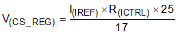
where
- I(IREF) is in A unit
- R(ICTRL) is in Ω unit
- V(CS_REG) is in V unit
The minimum voltage of V(CS_REF) is 50 mV typically to maintain the high accurate current output.
The final total output current for each channel can be calculated by using Equation 4 which is combination of Equation 1, Equation 2 and Equation 3.
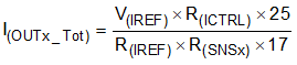
where
- V(IREF) = 1.235 V
- R(IREF) is in kΩ unit
- R(ICTRL) is in Ω unit
- R(SNSx) is in Ω unit
- I(OUTx_Tot) is in mA unit
The calculated result for I(OUTx_Tot) is 147.7 mA when R(IREF) is 12.3 kΩ, R(ICTRL) is 1000 Ω and R(SNSx) is 1Ω.