SLVSFE8 June 2021 TPS92633
PRODUCTION DATA
- 1 Features
- 2 Applications
- 3 Description
- 4 Revision History
- 5 Pin Configuration and Functions
- 6 Specifications
-
7 Detailed Description
- 7.1 Overview
- 7.2 Functional Block Diagram
- 7.3
Feature Description
- 7.3.1 Power Supply (SUPPLY)
- 7.3.2 Enable and Shutdown (EN)
- 7.3.3 Reference Current (IREF)
- 7.3.4 Constant-Current Output and Setting (INx)
- 7.3.5 Analog Current Control (ICTRL)
- 7.3.6 Thermal Sharing Resistor (OUTx and RESx)
- 7.3.7 PWM Control (PWMx)
- 7.3.8 Supply Control
- 7.3.9
Diagnostics
- 7.3.9.1 IREF Short-to-GND Detection
- 7.3.9.2 IREF Open Detection
- 7.3.9.3 LED Short-to-GND Detection
- 7.3.9.4 LED Open-Circuit Detection
- 7.3.9.5 Single LED Short-Circuit Detection (SLS_REF)
- 7.3.9.6 LED Open-Circuit and Single LED Short-Circuit Detection Enable (DIAGEN)
- 7.3.9.7 Low Dropout Operation
- 7.3.9.8 Over-Temperature Protection
- 7.3.10 FAULT Bus Output With One-Fails–All-Fail
- 7.3.11 FAULT Table
- 7.3.12 LED Fault Summary
- 7.3.13 IO Pins Inner Connection
- 7.4 Device Functional Modes
- 8 Application and Implementation
- 9 Power Supply Recommendations
- 10Layout
- 11Device and Documentation Support
- 12Mechanical, Packaging, and Orderable Information
Package Options
Mechanical Data (Package|Pins)
- PWP|20
Thermal pad, mechanical data (Package|Pins)
- PWP|20
Orderable Information
7.3.9.6 LED Open-Circuit and Single LED Short-Circuit Detection Enable (DIAGEN)
The TPS92633 device supports the DIAGEN pin with an accurate threshold to disable the LED open-circuit and single LED short-circuit diagnostic functions. The DIAGEN pin can be used to enable or disable LED open-circuit detection and single LED short-circuit detection based on SUPPLY pin voltage sensed by an external resistor divider as illustrated in Figure 7-11. When the voltage applied on DIAGEN pin is higher than the threshold VIH(DIAGEN), the device enables LED open-circuit and single LED short-circuit diagnosis. When V(DIAGEN) is lower than the threshold VIL(DIAGEN), the device disables LED open-circuit and single LED short-circuit detection.
Only LED open-circuit detection and single LED short-circuit detection can be disabled by pulling down the DIAGEN pin. The LED short-to-GND detection and over-temperature protection cannot be turned off by pulling down the DIAGEN pin. The SUPPLY threshold voltage can be calculated by using Equation 7.
 Figure 7-11 Application
Schematic for DIAGEN
Figure 7-11 Application
Schematic for DIAGEN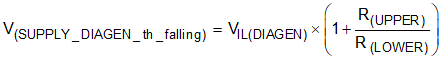
where
- VIL(DIAGEN) = 1.045 V (minimum)