SLVSFE8 June 2021 TPS92633
PRODUCTION DATA
- 1 Features
- 2 Applications
- 3 Description
- 4 Revision History
- 5 Pin Configuration and Functions
- 6 Specifications
-
7 Detailed Description
- 7.1 Overview
- 7.2 Functional Block Diagram
- 7.3
Feature Description
- 7.3.1 Power Supply (SUPPLY)
- 7.3.2 Enable and Shutdown (EN)
- 7.3.3 Reference Current (IREF)
- 7.3.4 Constant-Current Output and Setting (INx)
- 7.3.5 Analog Current Control (ICTRL)
- 7.3.6 Thermal Sharing Resistor (OUTx and RESx)
- 7.3.7 PWM Control (PWMx)
- 7.3.8 Supply Control
- 7.3.9
Diagnostics
- 7.3.9.1 IREF Short-to-GND Detection
- 7.3.9.2 IREF Open Detection
- 7.3.9.3 LED Short-to-GND Detection
- 7.3.9.4 LED Open-Circuit Detection
- 7.3.9.5 Single LED Short-Circuit Detection (SLS_REF)
- 7.3.9.6 LED Open-Circuit and Single LED Short-Circuit Detection Enable (DIAGEN)
- 7.3.9.7 Low Dropout Operation
- 7.3.9.8 Over-Temperature Protection
- 7.3.10 FAULT Bus Output With One-Fails–All-Fail
- 7.3.11 FAULT Table
- 7.3.12 LED Fault Summary
- 7.3.13 IO Pins Inner Connection
- 7.4 Device Functional Modes
- 8 Application and Implementation
- 9 Power Supply Recommendations
- 10Layout
- 11Device and Documentation Support
- 12Mechanical, Packaging, and Orderable Information
Package Options
Mechanical Data (Package|Pins)
- PWP|20
Thermal pad, mechanical data (Package|Pins)
- PWP|20
Orderable Information
8.2.1.2 Detailed Design Procedure
STEP 1: Determine the reference current setting resistor, R(IREF), by using Equation 8.
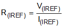
where
- V(IREF) = 1.235 V (typical)
- I(IREF) = 100 µA (recommended)
TI recommends 100 µA current for reference current, I(IREF) if the ICTRL resistor is placed in the same board with TPS92633. The calculated result for R(IREF) is 12.3 kΩ when I(IREF) = 100 µA.
STEP 2: Design the ICTRL resistor, R(ICTRL), for setting the regulation voltage, V(CS_REG) by using Equation 9.
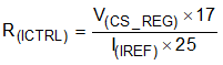
where
- V(CS_REG) = 100 mV (recommended)
- I(IREF) = 100 µA (recommended)
TI recommends 100 mV for reference voltage across current sensing resistor, R(SNSx) if the ICTRL pin is not used for driving off-board binning resistor or NTC resistor. The calculated result for R(ICTRL) is 680 Ω when V(CS_REG) = 100 mV.
STEP 3: Determine the current sensing resistor, R(SNSx), by using Equation 10.
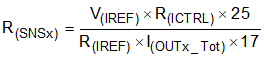
where
- V(IREF) = 1.235 V (typical)
- R(ICTRL) = 680 Ω
- R(IREF) = 12.3 kΩ
- I(OUTx_Tot) = 140 mA
According to design requirements, output current for each channel is same so that the R(SNS1) = R(SNS2) = R(SNS3) = 0.717 Ω. Two resistors in parallel are required to achieve equivalent 0.717-Ω resistance because 0.717 Ω is not a standard decade resistance value.
STEP 4: Design the current distribution between I(OUTx) and I(RESx), and calculate the current sharing resistor, R(RESx) by using Equation 11. The R(RESx) value actually decides the current distribution for I(OUTx) path and I(RESx) path, basic principle is to design the R(RESx) to consume appropriate 50% total power dissipation at typical supply operating voltage.
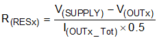
where
- V(SUPPLY) = 12 V (typical)
- I(OUTx_Tot) = 140 mA
The calculated result for R(RESx) resistor value including R(RES1), R(RES2) and R(RES3) is 75 Ω when V(OUTx) is typical 3 × 2.2 V = 6.6 V.
STEP 5: Design the single-LED short-circuit threshold voltage and calculate the value of R(SLS_REF) resistor for setting single-LED short-circuit threshold by using Equation 12.
The total forward voltage for three LEDs in serial is 3 × 2.5 V = 7.5-V maximum and 3 × 1.9 V = 5.7-V minimum. Once anyone of three LEDs is defective with short-circuit behavior, the total forward voltage for remaining two LEDs in serial is 2 × 2.5 V = 5-V maximum and 2 × 1.9 V = 3.8-V minimum. So the 5.3 V is selected to be threshold for single-LED short-circuit, V(SLS_th_falling).
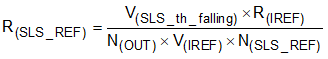
where
- V(IREF) = 1.235 V (typical)
- R(IREF) = 12.3 kΩ
- N(OUT) = 4
- N(SLS_REF) = 1
The calculated result for R(SLS_REF) is 13.3 kΩ for V(SLS_th_falling) is 5.34 V.
STEP 6: Design the threshold voltage of SUPPLY to enable the LED open-circuit and single-LED short-circuit diagnostics, and calculate voltage divider resistor value for R1 and R2 on DIAGEN pin.
The maximum forward voltage of LED-string is 3 × 2.5 V = 7.5 V. To avoid the open-circuit fault or single-LED short-circuit reported in low-dropout operation conditions, additional headroom between SUPPLY and OUTx needs to be considered. The TPS92633 device must disable open-circuit detection and single-LED short-circuit detection when the supply voltage is below LED-string maximum forward voltage plus V(OPEN_th_rising) and V(CS_REG). The voltage divider resistor, R1 and R2 value can be calculated by Equation 13.
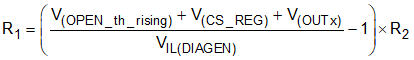
where
- V(OPEN_th_rising) = 210 mV (maximum)
- V(CS_REG) = 100 mV
- VIL(DIAGEN) = 1.045 V (minimum)
- R2 = 10 kΩ (recommended)
The calculated result for R1 is 64.9 kΩ when V(OUTx) maximum voltage is 7.5 V and V(CS_REG) is 100 mV.
STEP 7: Design the threshold voltage of SUPPLY to turn on and off each channel of LED, and calculate voltage divider resistor value for R3 and R4 on PWM input pin.
The minimum forward voltage of LED-string is 3 × 1.9 V = 5.7 V. To make sure the current output on each of LED-string is normal, each LED-string needs to be turned off when SUPPLY voltage is lower than LED minimum required forward voltage plus dropout voltage between INx to OUTx and V(CS_REG). The voltage divider resistor, R3 and R4 value can be calculated by Equation 14.
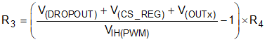
where
- V(DROPOUT) = 300 mV (typical)
- V(CS_REG) = 100 mV
- VIH(PWM) = 1.26 V (maximum)
- R4 = 10 kΩ (recommended)
The calculated result for R3 is 38.3 kΩ when V(OUTx) minimum voltage is 5.7 V and V(CS_REG) is 100 mV.