SLUSCX8C March 2019 – March 2021 TPS92682-Q1
PRODUCTION DATA
- 1 Features
- 2 Applications
- 3 Description
- 4 Revision History
- 5 Pin Configuration and Functions
- 6 Specifications
-
7 Detailed Description
- 7.1 Overview
- 7.2 Functional Block Diagram
- 7.3
Feature Description
- 7.3.1 Device Enable
- 7.3.2 Internal Regulator and Undervoltage Lockout (UVLO)
- 7.3.3 Oscillator
- 7.3.4 Spread Spectrum Function
- 7.3.5 Gate Driver
- 7.3.6 Rail-to-Rail Current Sense Amplifier
- 7.3.7 Transconductance Error Amplifier
- 7.3.8 Switch Current Sense
- 7.3.9 Slope Compensation
- 7.3.10 ILED Setting in CC Mode
- 7.3.11 Output Voltage Setting in CV Mode
- 7.3.12 PWM Dimming
- 7.3.13 P-Channel FET Gate Driver Output
- 7.3.14 Soft Start
- 7.3.15 Two-Phase Operation
- 7.3.16 Faults and Diagnostics
- 7.4 Device Functional Modes
- 7.5 Programming
- 7.6
TPS92682 Registers
- 7.6.1 EN Register
- 7.6.2 CFG1 Register
- 7.6.3 CFG2 Register
- 7.6.4 SWDIV Register
- 7.6.5 ISLOPE Register
- 7.6.6 FM Register
- 7.6.7 SOFTSTART Register
- 7.6.8 CH1IADJ Register
- 7.6.9 CH2IADJ Register
- 7.6.10 PWMDIV Register
- 7.6.11 CH1PWML Register
- 7.6.12 CH1PWMH Register
- 7.6.13 CH2PWML Register
- 7.6.14 CH2PWMH Register
- 7.6.15 ILIM Register
- 7.6.16 IFT Register
- 7.6.17 MFT Register
- 7.6.18 FLT1 Register (read only)
- 7.6.19 FLT2 Register (read only)
- 7.6.20 FEN1 Register
- 7.6.21 FEN2 Register
- 7.6.22 FLATEN Register
- 7.6.23 OV Register
- 7.6.24 LHCFG Register
- 7.6.25 LHCH1IADJ Register
- 7.6.26 LHCH2IADJ Register
- 7.6.27 LHCH1PWML Register
- 7.6.28 LHCH1PWMH Register
- 7.6.29 LHCH2PWML Register
- 7.6.30 LHCH2PWMH Register
- 7.6.31 LHILIM Register
- 7.6.32 LHIFT Register
- 7.6.33 LHMFT Register
- 7.6.34 LHFEN1 Register
- 7.6.35 LHFEN2 Register
- 7.6.36 LHFLATEN Register
- 7.6.37 LHOV Register
- 7.6.38 CAL Register
- 7.6.39 RESET Register
-
8 Application and Implementation
- 8.1 Application Information General Design Considerations
- 8.2 Application Information CC Mode
- 8.3 Typical Application CV Mode
- 8.4
Typical Application CC Mode
- 8.4.1 CC Boost Design Requirements
- 8.4.2
CC Boost Detailed Design Procedure
- 8.4.2.1 Calculating Duty Cycle
- 8.4.2.2 Setting Switching Frequency
- 8.4.2.3 Setting Dither Modulation Frequency
- 8.4.2.4 Inductor Selection
- 8.4.2.5 Output Capacitor Selection
- 8.4.2.6 Input Capacitor Selection
- 8.4.2.7 Main N-Channel MOSFET Selection
- 8.4.2.8 Rectifier Diode Selection
- 8.4.2.9 Setting ILED and Selecting RCS
- 8.4.2.10 Setting Switch Current Limit
- 8.4.2.11 Slope Compensation
- 8.4.2.12 Compensator Parameters
- 8.4.2.13 Overvoltage Protection
- 8.4.2.14 Series P-Channel MOSFET Selection
- 8.4.3 CC Buck-Boost Design Requirements
- 8.4.4
CC Buck-Boost Detailed Design Procedure
- 8.4.4.1 Calculating Duty Cycle
- 8.4.4.2 Setting Switching Frequency
- 8.4.4.3 Setting Dither Modulation Frequency
- 8.4.4.4 Inductor Selection
- 8.4.4.5 Output Capacitor Selection
- 8.4.4.6 Input Capacitor Selection
- 8.4.4.7 Main N-Channel MOSFET Selection
- 8.4.4.8 Rectifier Diode Selection
- 8.4.4.9 Setting ILED and Selecting RCS
- 8.4.4.10 Setting Switch Current Limit
- 8.4.4.11 Slope Compensation
- 8.4.4.12 Compensator Parameters
- 8.4.4.13 Overvoltage Protection
- 8.4.5 PWM Dimming Consideration
- 8.4.6 Application Curves
- 8.5
Typical Application CV Mode
- 8.5.1 CV Design Requirements
- 8.5.2
Detailed Design Procedure
- 8.5.2.1 Calculating Duty Cycle
- 8.5.2.2 Setting Switching Frequency
- 8.5.2.3 Setting Dither Modulation Frequency
- 8.5.2.4 Inductor Selection
- 8.5.2.5 Output Capacitor Selection
- 8.5.2.6 Input Capacitor Selection
- 8.5.2.7 Main N-Channel MOSFET Selection
- 8.5.2.8 Rectifier Diode Selection
- 8.5.2.9 Programming VOUT
- 8.5.2.10 Setting Switch Current Limit
- 8.5.2.11 Slope Compensation
- 8.5.2.12 Compensator Parameters
- 8.5.2.13 Overvoltage Protection
- 8.5.3 Application Curves
- 9 Power Supply Recommendations
- 10Layout
- 11Device and Documentation Support
- 12Mechanical, Packaging, and Orderable Information
Package Options
Mechanical Data (Package|Pins)
Thermal pad, mechanical data (Package|Pins)
Orderable Information
7.3.4 Spread Spectrum Function
The main clock of the TPS92682-Q1, CLKM, is generated using an internal ramp generator as shown in Figure 7-5. The internal ramp, RAMPCLKM, is compared with a reference voltage of VOSCREF to reset the ramp at the end of the clock period, TCLKM. When the reference voltage VOSCREF is constant (1 V), the main clock frequency is fixed. The frequency modulation of the main clock is achieved using an internal 8-bit digital counter DAC, and by modulating the reference voltage as shown in Figure 7-6. Both modulation frequency, FM, and the modulation magnitude, ΔFM, are programmable in the FM Register.
 Figure 7-5 Internal Ramp for CLKM Generation
 Figure 7-6 Internal Ramp Waveform
To achieve maximum attenuation in average-EMI scan, set a modulation frequency of FM ranging from 100 Hz to 1.2 kHz. A low modulating frequency has a small impact on the quasi-peak EMI scan. Set the modulation frequency to 10 KHz or higher to achieve attenuation for quasi-peak EMI measurements. A modulation frequency higher than the receiver resolution bandwidth (RBW) of 9 kHz impacts only the quasi-peak EMI scan and has little impact on the average EMI measurement. The TPS92682-Q1 device simplifies EMI compliance by providing the means to tune the modulation frequency, FM, and modulation magnitude, ΔFM, based on the measured EMI signature.
Equation 2 shows the relation between the channel switching frequency, fSW, and the desired modulation frequency FM.
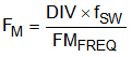
In Equation 2, DIV is the division factor between CLKM and the CHxCLK provided in SWDIV Register, and FMFREQ is the division factor given in the FM Register.
The output of the FM 8-bit digital counter always resets and starts from 1 V when a register write is performed to FM Register.