SLVSE03B April 2019 – February 2021 TPS929120-Q1
PRODUCTION DATA
- 1 Features
- 2 Applications
- 3 Description
- 4 Revision History
- 5 Pin Configuration and Functions
- 6 Specifications
-
7 Detailed Description
- 7.1 Overview
- 7.2 Functional Block Diagram
- 7.3
Feature Description
- 7.3.1 Device Bias and Power
- 7.3.2 Constant Current Output
- 7.3.3 PWM Dimming
- 7.3.4 On-chip 8-bit Analog-to-Digital Converter (ADC)
- 7.3.5
Diagnostic and Protection in Normal State
- 7.3.5.1 Fault Masking
- 7.3.5.2 Supply Undervoltage Lockout Diagnostics in Normal State
- 7.3.5.3 Low-Supply Warning Diagnostics in Normal State
- 7.3.5.4 Reference Diagnostics in Normal State
- 7.3.5.5 Pre-Thermal Warning and Overtemperature Protection in Normal State
- 7.3.5.6 Communication Loss Diagnostic in Normal State
- 7.3.5.7 LED Open-Circuit Diagnostics in Normal State
- 7.3.5.8 LED Short-circuit Diagnostics in Normal State
- 7.3.5.9 On-Demand Off-State Invisible Diagnostics
- 7.3.5.10 On-Demand Off-State Single-LED Short-Circuit (SS) Diagnostics
- 7.3.5.11 Automatic Single-LED Short-Circuit (AutoSS) Detection in Normal State
- 7.3.5.12 EEPROM CRC Error in Normal State
- 47
- 7.3.6
Diagnostic and Protection in Fail-Safe States
- 7.3.6.1 Fault Masking
- 7.3.6.2 Supply UVLO Diagnostics in Fail-Safe States
- 7.3.6.3 Low-supply Warning Diagnostics in Fail-Safe states
- 7.3.6.4 Reference Diagnostics at Fail-Safe States
- 7.3.6.5 Overtemperature Protection in Fail-Safe State
- 7.3.6.6 LED Open-circuit Diagnostics in Fail-Safe State
- 7.3.6.7 LED Short-circuit Diagnostics in Fail-safe State
- 7.3.6.8 EEPROM CRC Error in Fail-safe State
- 57
- 7.4 Device Functional Modes
- 7.5 Programming
- 7.6 Register Maps
- 8 Application and Implementation
- 9 Power Supply Recommendations
- 10Layout
- 11Device and Documentation Support
- 12Mechanical, Packaging, and Orderable Information
Package Options
Mechanical Data (Package|Pins)
- PWP|24
Thermal pad, mechanical data (Package|Pins)
- PWP|24
Orderable Information
7.3.2.2 64-Step Programmable High-Side Constant-Current Output
TPS929120-Q1 has 12 channels of high-side current sources. Each channel has its own enable configuration register CONF_ENCHx. Setting CONF_ENCHx to 1 enables the channel output; clearing the register to 0 disables the channel output. To completely turn off the channel current, user can clear channel enable bit CONF_ENCHx to 0. Upon power up, CONF_ENCHx is automatically reset to 0 to avoid unwanted blinking.
Each OUTx channel supports individual 64-step programmable current setting, also known as dot correction (DC). The DC feature can be used to set binning values for output LEDs or to calibrate the LEDs to achieve high brightness homogeneity based on external visual system to further save binning cost. The 6-bit register CONF_IOUTx sets the current independently, where x is the channel number from 0 to 11. The OUTx current can be calculated with Equation 2
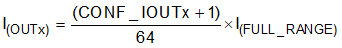
where
- CONF_IOUTx is programmable from 0 to 63
- x is from 0 to 11 for different output channel
- I(FULL_RANGE) can be calculated with Equation 1