SLVSFZ4A December 2020 – February 2021 TPS929121-Q1
PRODUCTION DATA
- 1 Features
- 2 Applications
- 3 Description
- 4 Revision History
- 5 Device Comparison Table
- 6 Pin Configuration and Functions
- 7 Specifications
-
8 Detailed Description
- 8.1 Overview
- 8.2 Functional Block Diagram
- 8.3
Feature Description
- 8.3.1 Device Bias and Power
- 8.3.2 Constant Current Output
- 8.3.3 PWM Dimming
- 8.3.4 On-chip 8-bit Analog-to-Digital Converter (ADC)
- 8.3.5
Diagnostic and Protection in Normal State
- 8.3.5.1 Fault Masking
- 8.3.5.2 Supply Undervoltage Lockout Diagnostics in Normal State
- 8.3.5.3 Low-Supply Warning Diagnostics in Normal State
- 8.3.5.4 Reference Diagnostics in Normal State
- 8.3.5.5 Pre-Thermal Warning and Overtemperature Protection in Normal State
- 8.3.5.6 Communication Loss Diagnostic in Normal State
- 8.3.5.7 LED Open-Circuit Diagnostics in Normal State
- 8.3.5.8 LED Short-Circuit Diagnostics in Normal State
- 8.3.5.9 On-Demand Off-State Invisible Diagnostics
- 8.3.5.10 On-Demand Off-State Single-LED Short-Circuit (SS) Diagnostics
- 8.3.5.11 Automatic Single-LED Short-Circuit (AutoSS) Detection in Normal State
- 8.3.5.12 EEPROM CRC Error in Normal State
- 48
- 8.3.6
Diagnostic and Protection in Fail-Safe States
- 8.3.6.1 Fault Masking
- 8.3.6.2 Supply UVLO Diagnostics in Fail-Safe States
- 8.3.6.3 Low-supply Warning Diagnostics in Fail-Safe states
- 8.3.6.4 Reference Diagnostics at Fail-Safe States
- 8.3.6.5 Overtemperature Protection in Fail-Safe State
- 8.3.6.6 LED Open-circuit Diagnostics in Fail-Safe State
- 8.3.6.7 LED Short-circuit Diagnostics in Fail-Safe State
- 8.3.6.8 EEPROM CRC Error in Fail-safe State
- 58
- 8.4 Device Functional Modes
- 8.5 Programming
- 8.6 Register Maps
- 9 Application and Implementation
- 10Power Supply Recommendations
- 11Layout
- 12Device and Documentation Support
- 13Mechanical, Packaging, and Orderable Information
Package Options
Mechanical Data (Package|Pins)
- PWP|24
Thermal pad, mechanical data (Package|Pins)
- PWP|24
Orderable Information
8.5.4.3 EEPROM Register Access and Burn
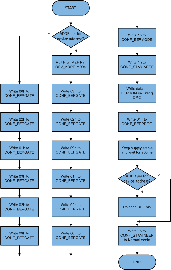
After selecting the target TPS929121-Q1 for EEPROM burning, the master controller must send a serial data bytes to register CONF_EEPGATE, set 1 to CONF_EEPMODE and set 1 to register CONF_STAYINEEP one by one in below sequency to finally enable the EEPROM register access. Each data written must be a single-byte operation instead of burst-mode operation.
Chip is selected by pulling REF pin high, below instruction is required to access the EEPROM register.
- Write 09h, 02h, 09h, 01h, 02h, 00h to 8-bit register CONF_EEPGATE one-byte by one-byte sequentially.
- Write 1 to 1-bit register CONF_EEPMODE.
- Write 1 to 1-bit register CONF_STAYINEEP.
Chip is selected by ADDR pins configuration, below instruction is required to access the EEPROM register.
- Write 00h, 02h, 01h, 09h, 02h, 09h to 8-bit register CONF_EEPGATE one-byte by one-byte sequentially.
- Write 1 to 1-bit register CONF_EEPMODE.
- Write 1 to 1-bit register CONF_STAYINEEP.
The EEPROM registers of the TPS929121-Q1 can be overwritten after the access enabled. Then master controller can set CONF_EEPPROG to 1 to start the burning of all the EEPROM register. The data for EEPROM register is only stored in EEPROM shadow register without burning into true EEPROM cell before setting CONF_EEPPROG to 1. The data is lost after POR cycle if it is not burnt to EEPROM cell. All EEPROM shadow registers need to be written to target value before burning. The CONF_EEPPROG automatically returns to 0 at the next clock cycle. The programming takes around 200 ms and flag register FLAG_PROGREADY is 0 during programming. It is important to keep device power supply stable for at least 200 ms after writing 1 to CONF_EEPPROG to make sure solid and robust burning. After programming is done, the FLAG_PROGREADY is automatically set to 1. The detail flow chart is described in Figure 8-18.
The EEPROM cells for TPS929121-Q1 can be overwritten and burnt for up to 1000 times. The one time EEPROM burning is counted once the register CONF_EEPPROG is set to 1 even though the EEPROM data is not changed at all.
 Figure 8-18 Programming Sequence