DLPS039F December 2015 – April 2019 TPS99000-Q1
PRODUCTION DATA.
- 1 Features
- 2 Applications
- 3 Description
- 4 Revision History
- 5 Pin Configuration and Functions
-
6 Specifications
- 6.1 Absolute Maximum Ratings
- 6.2 ESD Ratings
- 6.3 Recommended Operating Conditions
- 6.4 Thermal Information
- 6.5 Electrical Characteristics - Transimpedance Amplifier Parameters
- 6.6 Electrical Characteristics - Digital to Analog Converters
- 6.7 Electrical Characteristics - Analog to Digital Converter
- 6.8 Electrical Characteristics - FET Gate Drivers
- 6.9 Electrical Characteristics - Photo Comparator
- 6.10 Electrical Characteristics - Voltage Regulators
- 6.11 Electrical Characteristics - Temperature and Voltage Monitors
- 6.12 Electrical Characteristics - Current Consumption
- 6.13 Power-Up Timing Requirements
- 6.14 Power-Down Timing Requirements
- 6.15 Timing Requirements - Sequencer Clock
- 6.16 Timing Requirements - Host / Diagnostic Port SPI Interface
- 6.17 Timing Requirements - ADC Interface
- 6.18 Switching Characteristics
-
7 Detailed Description
- 7.1 Overview
- 7.2 Functional Block Diagram
- 7.3
Feature Description
- 7.3.1
Illumination Control
- 7.3.1.1 Illumination System High Dynamic Range Dimming Overview
- 7.3.1.2 Illumination Control Loop
- 7.3.1.3 Continuous Mode Operation
- 7.3.1.4
Discontinuous Mode Operation
- 7.3.1.4.1 Discontinuous Mode Pulse Width Limit
- 7.3.1.4.2 COMPOUT_LOW Timer in Discontinuous Operation
- 7.3.1.4.3 Dimming Within Discontinuous Operation Range
- 7.3.1.4.4 Multiple Pulse Heights to Increase Bit Depth
- 7.3.1.4.5 TIA Gain Adjustment
- 7.3.1.4.6 Current Limit in Discontinuous Mode
- 7.3.1.4.7 CMODE Big Cap Mode in Discontinuous Operation
- 7.3.2 Over-Brightness Detection
- 7.3.3 Analog to Digital Converter
- 7.3.4 Power Sequencing and Monitoring
- 7.3.5 DMD Mirror Voltage Regulator
- 7.3.6 Low Dropout Regulators
- 7.3.7 System Monitoring Features
- 7.3.8 Communication Ports
- 7.3.1
Illumination Control
- 7.4 Device Functional Modes
- 7.5 Register Maps
- 8 Application and Implementation
- 9 Power Supply Recommendations
- 10Layout
- 11Device and Documentation Support
- 12Mechanical, Packaging, and Orderable Information
Package Options
Mechanical Data (Package|Pins)
- PZP|100
Thermal pad, mechanical data (Package|Pins)
- PZP|100
Orderable Information
7.3.1.3.5 Continuous Mode Current Limit
In continuous mode, a current limit feature prevents damage to LEDs if the requested light output cannot be achieved within LED current specifications. This could happen due to high temperature, or when an LED ages and requires more current to achieve the same brightness. Systems should be designed with sufficient thermal and LED life time margin that this would not happen in practice.
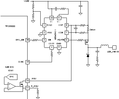
The control scheme utilizes the built in current limit feature of the LM3409 device plus a 10-bit DAC based adjustment feature included in the TPS99000-Q1. This serves as an alternate limit for the current for the LEDs – inductor drive will be disabled if either the current limit is met or if the photo feedback limit is met, whichever is lower. This peak current limit is configurable on a per LED basis, and is in use during the light-on active periods only. (During blanking periods, this same structure is used to control the blanking current, but different values are loaded onto the ILIM DAC).
The schematic for the current adjustment mechanism is shown in Figure 19.
 Figure 19. IADJ Peak Current Limit Schematic
 By design, the LM3409 seeks to create a zero voltage difference between the CSP and CSN pins when IADJ pin is held low and system is operating in peak current limit mode. If the CSP pin voltage is higher than the CSN pin voltage, the PGATE driver is held high (PFET off).
When the ILIM DAC is set to a non-zero voltage, a current is established on the IADJ line of the TPS99000-Q1 device, which pulls the voltage of the CSP pin downward. If the LM3409 device is enabled and PFET drive not held off by state of the COFF pin, then the current will go up until the voltage across the sense resistor is such that the CSN pin is equal to or greater than the voltage on the CSP pin, at which point the PFET is turned off.
Care must be taken with the routing of the IADJ pin of the TPS99000-Q1 to insure that it is well isolated from noisy switching nodes, such as the PFET drain node.