DLPS039F December 2015 – April 2019 TPS99000-Q1
PRODUCTION DATA.
- 1 Features
- 2 Applications
- 3 Description
- 4 Revision History
- 5 Pin Configuration and Functions
-
6 Specifications
- 6.1 Absolute Maximum Ratings
- 6.2 ESD Ratings
- 6.3 Recommended Operating Conditions
- 6.4 Thermal Information
- 6.5 Electrical Characteristics - Transimpedance Amplifier Parameters
- 6.6 Electrical Characteristics - Digital to Analog Converters
- 6.7 Electrical Characteristics - Analog to Digital Converter
- 6.8 Electrical Characteristics - FET Gate Drivers
- 6.9 Electrical Characteristics - Photo Comparator
- 6.10 Electrical Characteristics - Voltage Regulators
- 6.11 Electrical Characteristics - Temperature and Voltage Monitors
- 6.12 Electrical Characteristics - Current Consumption
- 6.13 Power-Up Timing Requirements
- 6.14 Power-Down Timing Requirements
- 6.15 Timing Requirements - Sequencer Clock
- 6.16 Timing Requirements - Host / Diagnostic Port SPI Interface
- 6.17 Timing Requirements - ADC Interface
- 6.18 Switching Characteristics
-
7 Detailed Description
- 7.1 Overview
- 7.2 Functional Block Diagram
- 7.3
Feature Description
- 7.3.1
Illumination Control
- 7.3.1.1 Illumination System High Dynamic Range Dimming Overview
- 7.3.1.2 Illumination Control Loop
- 7.3.1.3 Continuous Mode Operation
- 7.3.1.4
Discontinuous Mode Operation
- 7.3.1.4.1 Discontinuous Mode Pulse Width Limit
- 7.3.1.4.2 COMPOUT_LOW Timer in Discontinuous Operation
- 7.3.1.4.3 Dimming Within Discontinuous Operation Range
- 7.3.1.4.4 Multiple Pulse Heights to Increase Bit Depth
- 7.3.1.4.5 TIA Gain Adjustment
- 7.3.1.4.6 Current Limit in Discontinuous Mode
- 7.3.1.4.7 CMODE Big Cap Mode in Discontinuous Operation
- 7.3.2 Over-Brightness Detection
- 7.3.3 Analog to Digital Converter
- 7.3.4 Power Sequencing and Monitoring
- 7.3.5 DMD Mirror Voltage Regulator
- 7.3.6 Low Dropout Regulators
- 7.3.7 System Monitoring Features
- 7.3.8 Communication Ports
- 7.3.1
Illumination Control
- 7.4 Device Functional Modes
- 7.5 Register Maps
- 8 Application and Implementation
- 9 Power Supply Recommendations
- 10Layout
- 11Device and Documentation Support
- 12Mechanical, Packaging, and Orderable Information
Package Options
Mechanical Data (Package|Pins)
- PZP|100
Thermal pad, mechanical data (Package|Pins)
- PZP|100
Orderable Information
7.3.1.3 Continuous Mode Operation
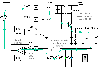
When operating in continuous mode (continuous light output mode) a hysteretic control scheme is utilized. Real-time analog light amplitude measurements are used in the photo feedback loop to maintain a target light level. Figure 8 highlights the photo feedback control loop path in the driver for continuous mode.
 Figure 8. Continuous Mode Photo Feedback Path
 The on-chip analog comparator of the TPS99000-Q1 is used to compare desired target LED light amplitude to actual LED light output voltage from the photodiode TIA circuit. When the light output is below the threshold (set by the 12-bit photo feedback DAC output), the comparator will output a high level, causing DRV_EN to go high, which creates a connection from the power rail to the LED drive inductor to be made through the LED drive PFET. This connection will cause current flow to increase through the inductor. This current flows through an LED when its FET is enabled. When the light value goes above the threshold, DRV_EN goes low and the PFET is turned off, breaking the connection to the power rail with very little delay. Once the light level drops back below the threshold, DRV_EN goes high again and the PFET is turned back on, delivering more power to the LED. This process repeats as long as the LED circuit is enabled.
Hysteretic control results in ripple in the LED current. The amplitude and frequency of this ripple is a function of inductor inductance, input voltage, comparator hysteresis, and loop latency. An advantage of this hysteretic control approach is unconditional stability of the control loop.
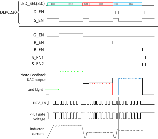
Figure 9 shows the continuous mode signals and light output for a red, green, and blue bit slice. The signals, including LED_SEL(3:0), D_EN, S_EN1, and S_EN2, are sent from the DLPC230-Q1.
 Figure 9. Continuous Mode Signal Example
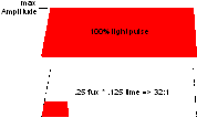
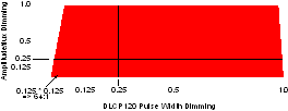
 In continuous mode, dimming is accomplished through a combination of amplitude/flux dimming and pulse time attenuation. Amplitude dimming is done by adjusting the photo feedback DAC output and TIA feedback gain. Time attenuation is accomplished by adjusting the length of shunt enable (S_EN from DLPC230-Q1) and drive enable (D_EN from DLPC230-Q1) (see Figure 10). Figure 10 shows an example with a 100% bit and a bit with time and amplitude attenuation to achieve 32:1 dimming. Figure 11 is a more generic example showing how many different dimming levels can be achieved with combinations of time and amplitude dimming.
 Figure 10. Continuous Mode Dimming Illustration 1
  Figure 11. Continuous Mode Dimming Illustration 2