DLPS039F December 2015 – April 2019 TPS99000-Q1
PRODUCTION DATA.
- 1 Features
- 2 Applications
- 3 Description
- 4 Revision History
- 5 Pin Configuration and Functions
-
6 Specifications
- 6.1 Absolute Maximum Ratings
- 6.2 ESD Ratings
- 6.3 Recommended Operating Conditions
- 6.4 Thermal Information
- 6.5 Electrical Characteristics - Transimpedance Amplifier Parameters
- 6.6 Electrical Characteristics - Digital to Analog Converters
- 6.7 Electrical Characteristics - Analog to Digital Converter
- 6.8 Electrical Characteristics - FET Gate Drivers
- 6.9 Electrical Characteristics - Photo Comparator
- 6.10 Electrical Characteristics - Voltage Regulators
- 6.11 Electrical Characteristics - Temperature and Voltage Monitors
- 6.12 Electrical Characteristics - Current Consumption
- 6.13 Power-Up Timing Requirements
- 6.14 Power-Down Timing Requirements
- 6.15 Timing Requirements - Sequencer Clock
- 6.16 Timing Requirements - Host / Diagnostic Port SPI Interface
- 6.17 Timing Requirements - ADC Interface
- 6.18 Switching Characteristics
-
7 Detailed Description
- 7.1 Overview
- 7.2 Functional Block Diagram
- 7.3
Feature Description
- 7.3.1
Illumination Control
- 7.3.1.1 Illumination System High Dynamic Range Dimming Overview
- 7.3.1.2 Illumination Control Loop
- 7.3.1.3 Continuous Mode Operation
- 7.3.1.4
Discontinuous Mode Operation
- 7.3.1.4.1 Discontinuous Mode Pulse Width Limit
- 7.3.1.4.2 COMPOUT_LOW Timer in Discontinuous Operation
- 7.3.1.4.3 Dimming Within Discontinuous Operation Range
- 7.3.1.4.4 Multiple Pulse Heights to Increase Bit Depth
- 7.3.1.4.5 TIA Gain Adjustment
- 7.3.1.4.6 Current Limit in Discontinuous Mode
- 7.3.1.4.7 CMODE Big Cap Mode in Discontinuous Operation
- 7.3.2 Over-Brightness Detection
- 7.3.3 Analog to Digital Converter
- 7.3.4 Power Sequencing and Monitoring
- 7.3.5 DMD Mirror Voltage Regulator
- 7.3.6 Low Dropout Regulators
- 7.3.7 System Monitoring Features
- 7.3.8 Communication Ports
- 7.3.1
Illumination Control
- 7.4 Device Functional Modes
- 7.5 Register Maps
- 8 Application and Implementation
- 9 Power Supply Recommendations
- 10Layout
- 11Device and Documentation Support
- 12Mechanical, Packaging, and Orderable Information
Package Options
Mechanical Data (Package|Pins)
- PZP|100
Thermal pad, mechanical data (Package|Pins)
- PZP|100
Orderable Information
7.3.1.4.3 Dimming Within Discontinuous Operation Range
When operating in discontinuous mode, two methods of dimming are used concurrently to reduce brightness of the display:
- Amplitude dimming using the photo feedback DAC settings.
- Controlling the number of pulses per bit slice (via commands to DLPC230-Q1, selecting specific lookup table data).
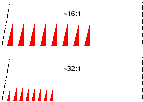
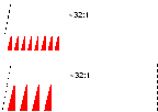
Figure 25 is an example of the brightest LUT data table having 8 pulses per LSB (smallest bit slice). The LED pulse height is modulated to achieve a 2:1 dimming ratio while still maintaining 8 pulses per LSB. To allow for a seamless transition to lower dimming levels, a change to 4 pulses per LSB plus higher LED amplitude is made as illustrated in Figure 26. The total light generated in both cases in Figure 26 is approximately equal. A system calibration is used to determine this ½ LED amplitude photo feedback DAC setting.
 Figure 25. 2:1 Dimming Within a Sequence
  Figure 26. Discontinuous Operation Pulse Count Change
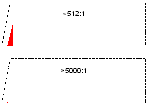
 As a smooth dimming (brightness going down) sequence continues, the process above eventually results in using a 1 pulse per LSB. Amplitude dimming is used to dim to the absolute minimum display brightness level as illustrated in Figure 27.
 Figure 27. Discontinuous Dimming with One Pulse Per LSB Sequence
 As shown in Figure 27, once a single pulse-per-LSB is selected, all remaining dimming must occur using only pulse height threshold reduction.