DLPS039F December 2015 – April 2019 TPS99000-Q1
PRODUCTION DATA.
- 1 Features
- 2 Applications
- 3 Description
- 4 Revision History
- 5 Pin Configuration and Functions
-
6 Specifications
- 6.1 Absolute Maximum Ratings
- 6.2 ESD Ratings
- 6.3 Recommended Operating Conditions
- 6.4 Thermal Information
- 6.5 Electrical Characteristics - Transimpedance Amplifier Parameters
- 6.6 Electrical Characteristics - Digital to Analog Converters
- 6.7 Electrical Characteristics - Analog to Digital Converter
- 6.8 Electrical Characteristics - FET Gate Drivers
- 6.9 Electrical Characteristics - Photo Comparator
- 6.10 Electrical Characteristics - Voltage Regulators
- 6.11 Electrical Characteristics - Temperature and Voltage Monitors
- 6.12 Electrical Characteristics - Current Consumption
- 6.13 Power-Up Timing Requirements
- 6.14 Power-Down Timing Requirements
- 6.15 Timing Requirements - Sequencer Clock
- 6.16 Timing Requirements - Host / Diagnostic Port SPI Interface
- 6.17 Timing Requirements - ADC Interface
- 6.18 Switching Characteristics
-
7 Detailed Description
- 7.1 Overview
- 7.2 Functional Block Diagram
- 7.3
Feature Description
- 7.3.1
Illumination Control
- 7.3.1.1 Illumination System High Dynamic Range Dimming Overview
- 7.3.1.2 Illumination Control Loop
- 7.3.1.3 Continuous Mode Operation
- 7.3.1.4
Discontinuous Mode Operation
- 7.3.1.4.1 Discontinuous Mode Pulse Width Limit
- 7.3.1.4.2 COMPOUT_LOW Timer in Discontinuous Operation
- 7.3.1.4.3 Dimming Within Discontinuous Operation Range
- 7.3.1.4.4 Multiple Pulse Heights to Increase Bit Depth
- 7.3.1.4.5 TIA Gain Adjustment
- 7.3.1.4.6 Current Limit in Discontinuous Mode
- 7.3.1.4.7 CMODE Big Cap Mode in Discontinuous Operation
- 7.3.2 Over-Brightness Detection
- 7.3.3 Analog to Digital Converter
- 7.3.4 Power Sequencing and Monitoring
- 7.3.5 DMD Mirror Voltage Regulator
- 7.3.6 Low Dropout Regulators
- 7.3.7 System Monitoring Features
- 7.3.8 Communication Ports
- 7.3.1
Illumination Control
- 7.4 Device Functional Modes
- 7.5 Register Maps
- 8 Application and Implementation
- 9 Power Supply Recommendations
- 10Layout
- 11Device and Documentation Support
- 12Mechanical, Packaging, and Orderable Information
Package Options
Mechanical Data (Package|Pins)
- PZP|100
Thermal pad, mechanical data (Package|Pins)
- PZP|100
Orderable Information
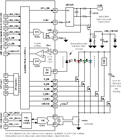
7.3.1.2 Illumination Control Loop
Figure 7 shows the illumination control loop. This loop consists of the following features:
- An external buck controller (LM3409) and related discrete components which control the main LED drive PFET and controls and limits peak current using a high side sense circuit. This circuit creates a controlled current source that drives the LED high side connection (LED_ANODE).
- A 10-bit peak current limit (ILIM) adjustment DAC included in the TPS99000-Q1.
- Synchronization logic for external LED drive buck. SYNC pin to override the controlled off time pin of external device, and DRV_EN to control enable of external device.
- High speed comparator, used to compare photo feedback signal to programmable reference.
- 12-bit photo feedback comparison DAC. Sets reference for LED light pulse peak threshold in both continuous and discontinuous operating modes.
- A high speed, low noise, wide dynamic range transimpedance amplifier (TIA1) used for real time photo feedback. Includes support for 0.75 V to 288 V/mA gains, with 14 discrete gain steps and additional RGB specific trim of 1.0 to 0.2 gain. (Two TIAs included. TIA1 is dedicated to illumination control function).
- Negative LDO for cost effective reverse bias of photodiodes.
- 12-bit ADC, with differential input dedicated to low side current measurements.
- External FET gate drivers for RGB channel selection and two shunt path selections. Shunt paths provide a conduction path around the LEDs. These paths are used to control inductor current while LEDs are not emitting light. Control logic and firmware establishes appropriate current levels in inductor prior to enabling of LED during gaps between light pulses.
 Figure 7. Illumination Control Loop