DLPS039F December 2015 – April 2019 TPS99000-Q1
PRODUCTION DATA.
- 1 Features
- 2 Applications
- 3 Description
- 4 Revision History
- 5 Pin Configuration and Functions
-
6 Specifications
- 6.1 Absolute Maximum Ratings
- 6.2 ESD Ratings
- 6.3 Recommended Operating Conditions
- 6.4 Thermal Information
- 6.5 Electrical Characteristics - Transimpedance Amplifier Parameters
- 6.6 Electrical Characteristics - Digital to Analog Converters
- 6.7 Electrical Characteristics - Analog to Digital Converter
- 6.8 Electrical Characteristics - FET Gate Drivers
- 6.9 Electrical Characteristics - Photo Comparator
- 6.10 Electrical Characteristics - Voltage Regulators
- 6.11 Electrical Characteristics - Temperature and Voltage Monitors
- 6.12 Electrical Characteristics - Current Consumption
- 6.13 Power-Up Timing Requirements
- 6.14 Power-Down Timing Requirements
- 6.15 Timing Requirements - Sequencer Clock
- 6.16 Timing Requirements - Host / Diagnostic Port SPI Interface
- 6.17 Timing Requirements - ADC Interface
- 6.18 Switching Characteristics
-
7 Detailed Description
- 7.1 Overview
- 7.2 Functional Block Diagram
- 7.3
Feature Description
- 7.3.1
Illumination Control
- 7.3.1.1 Illumination System High Dynamic Range Dimming Overview
- 7.3.1.2 Illumination Control Loop
- 7.3.1.3 Continuous Mode Operation
- 7.3.1.4
Discontinuous Mode Operation
- 7.3.1.4.1 Discontinuous Mode Pulse Width Limit
- 7.3.1.4.2 COMPOUT_LOW Timer in Discontinuous Operation
- 7.3.1.4.3 Dimming Within Discontinuous Operation Range
- 7.3.1.4.4 Multiple Pulse Heights to Increase Bit Depth
- 7.3.1.4.5 TIA Gain Adjustment
- 7.3.1.4.6 Current Limit in Discontinuous Mode
- 7.3.1.4.7 CMODE Big Cap Mode in Discontinuous Operation
- 7.3.2 Over-Brightness Detection
- 7.3.3 Analog to Digital Converter
- 7.3.4 Power Sequencing and Monitoring
- 7.3.5 DMD Mirror Voltage Regulator
- 7.3.6 Low Dropout Regulators
- 7.3.7 System Monitoring Features
- 7.3.8 Communication Ports
- 7.3.1
Illumination Control
- 7.4 Device Functional Modes
- 7.5 Register Maps
- 8 Application and Implementation
- 9 Power Supply Recommendations
- 10Layout
- 11Device and Documentation Support
- 12Mechanical, Packaging, and Orderable Information
Package Options
Mechanical Data (Package|Pins)
- PZP|100
Thermal pad, mechanical data (Package|Pins)
- PZP|100
Orderable Information
7.3.6 Low Dropout Regulators
The TPS99000-Q1 includes four low drop out regulators, dedicated to specific internal functions:
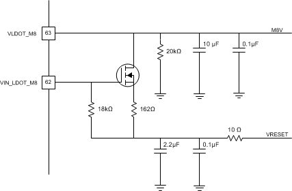
- A fixed –8 V negative regulator for photodiode reverse biasing (VIN_LDOT_M8 input, VLDOT_M8 output)
- A 5 V output regulator for internal analog circuits (VIN_LDOT_5V input, VLDOT_5V output)
- A 3.3 V output regulator for internal analog (VIN_LDOT_3P3V input, VLDOT_3P3V output)
- A 3.3 V output regulator dedicated to the ADC block (VIN_LDOA_3P3 input, VLDOA_3P3 output)
The positive output LDO regulators are all designed to operate from the same nominal 6 V input as is needed by the LED selection FET gate driver supply input, DRVR_PWR and the DMD mirror voltage regulator, VIN_DRST. However, care must be taken to isolate the sensitive analog circuit power supply inputs from switching noise, through dedicated sub-planes and supply filtering techniques. Noise on the analog supply rails will directly impact system dimming range performance, limiting stable operation at low brightness levels.
The negative 8 V LDO is designed to use the DMD_VRESET power rail as its power source. (Note that this usage implies that the TIA/photodiode path will not be available for use until the DMD is in a powered up state.)
 Figure 37. Negative 8 V LDO Circuit
 CAUTION
Applications that do not use a photodiode do not require the -8 V regulator. VLDOT_M8 and VIN_LDOT_M8 may be left disconnected if the option in the DLPC230 SW to prevent enabling of the –8 V LDO is selected. If these pins are not connected, care must be taken to confirm that the -8 V LDO is not enabled. If this regulator is enabled while the pins are disconnected, permanent damage may be caused to the device.