SLVSGS3B april 2022 – august 2023 TPSI3052
PRODUCTION DATA
- 1
- 1 Features
- 2 Applications
- 3 Description
- 4 Revision History
- 5 Pin Configuration and Functions
-
6 Specifications
- 6.1 Absolute Maximum Ratings
- 6.2 ESD Ratings
- 6.3 Recommended Operating Conditions
- 6.4 Thermal Information
- 6.5 Power Ratings
- 6.6 Insulation Specifications
- 6.7 Safety-Related Certifications
- 6.8 Safety Limiting Values
- 6.9 Electrical Characteristics
- 6.10 Switching Characteristics
- 6.11 Insulation Characteristic Curves
- 6.12 Typical Characteristics
- 7 Parameter Measurement Information
- 8 Detailed Description
-
9 Application and Implementation
- 9.1 Application Information
- 9.2
Typical Application
- 9.2.1 Design Requirements
- 9.2.2
Detailed Design Procedure
- 9.2.2.1 Two-Wire or Three-Wire Mode Selection
- 9.2.2.2 Standard Enable, One-Shot Enable
- 9.2.2.3 CDIV1, CDIV2 Capacitance
- 9.2.2.4 RPXFR Selection
- 9.2.2.5 CVDDP Capacitance
- 9.2.2.6 Gate Driver Output Resistor
- 9.2.2.7 Start-up Time and Recovery Time
- 9.2.2.8 Supplying Auxiliary Current, IAUX From VDDM
- 9.2.2.9 VDDM Ripple Voltage
- 9.2.3 Application Curves
- 9.3 Power Supply Recommendations
- 9.4 Layout
- 10Device and Documentation Support
- 11Mechanical, Packaging, and Orderable Information
Package Options
Mechanical Data (Package|Pins)
- DWZ|8
Thermal pad, mechanical data (Package|Pins)
Orderable Information
9.4.2 Layout Example
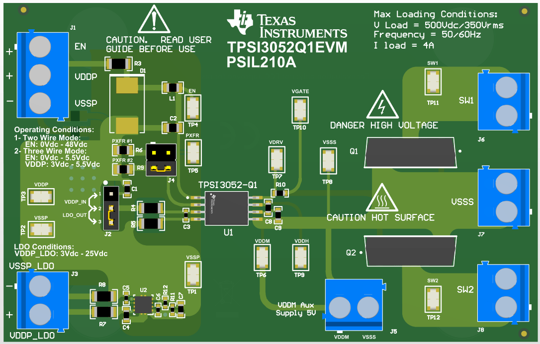
Figure 9-12 shows a PCB layout example with the signals and key components labeled.
 Figure 9-12 3-D PCB View
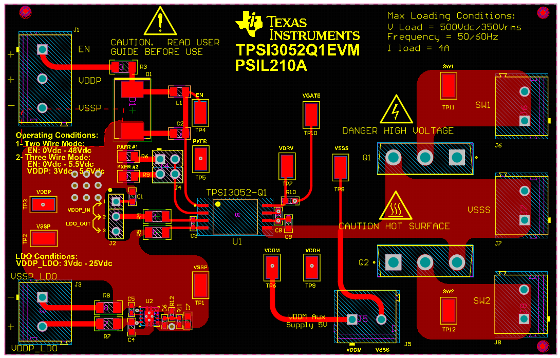
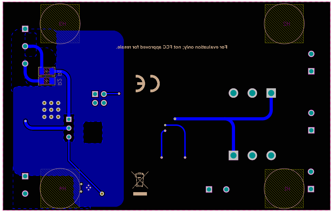
Figure 9-13 and Figure 9-14 show the top and bottom layer traces and copper.
 Figure 9-13 Top Layer
 Figure 9-14 Bottom Layer