SNVSBT8 March 2021 TPSM13604H
PRODUCTION DATA
- 1 Features
- 2 Applications
- 3 Description
- 4 Revision History
- 5 Pin Configuration and Functions
- 6 Specifications
- 7 Detailed Description
-
8 Application and Implementation
- 8.1 Application Information
- 8.2
Typical Application
- 8.2.1 Design Requirements
- 8.2.2
Detailed Design Procedure
- 8.2.2.1 Design Steps for the TPSM13604 Application
- 8.2.3 Application Curve
- 9 Power Supply Recommendations
- 10Layout
- 11Device and Documentation Support
- 12Mechanical, Packaging, and Orderable Information
Package Options
Mechanical Data (Package|Pins)
- NDW|7
Thermal pad, mechanical data (Package|Pins)
Orderable Information
10.1.1 Power Module SMT Guidelines
The following recommendations are for a standard module surface mount assembly:
- Land Pattern – Follow the PCB land pattern with either soldermask defined or non-soldermask defined pads.
- Stencil Aperture
- For the exposed die attach pad (DAP), adjust the stencil for approximately 80% coverage of the PCB land pattern.
- For all other I/O pads, use a 1:1 ratio between the aperture and the land pattern recommendation.
- Solder Paste – Use a standard SAC Alloy such as SAC 305, type 3 or higher.
- Stencil Thickness – 0.125 mm to 0.15 mm
- Reflow - Refer to solder paste supplier recommendation and optimized per board size and density.
- Refer to AN Design Summary LMZ1xxx and LMZ2xxx Power Modules Family for reflow information.
- Maximum number of reflows allowed is one.
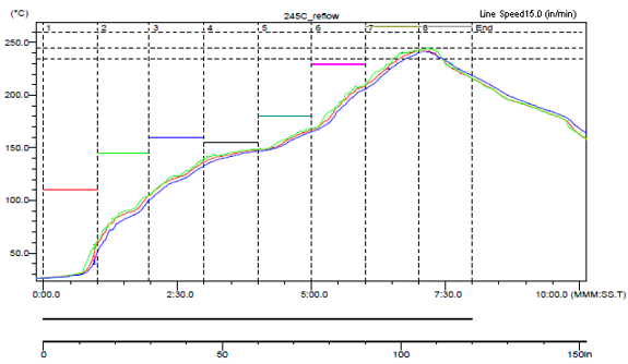
 Figure 10-1 Sample Reflow Profile
Table 10-1 Sample Reflow Profile Table
| PROBE | MAX TEMP (°C) | REACHED MAX TEMP | TIME ABOVE 235°C | REACHED 235°C | TIME ABOVE 245°C | REACHED 245°C | TIME ABOVE 260°C | REACHED 260°C |
|---|---|---|---|---|---|---|---|---|
| 1 | 242.5 | 6.58 | 0.49 | 6.39 | 0 | – | 0 | – |
| 2 | 242.5 | 7.1 | 0.55 | 6.31 | 0 | 7.1 | 0 | – |
| 3 | 241 | 7.09 | 0.42 | 6.44 | 0 | – | 0 | – |