SNVSBF6B October 2019 – December 2020 TPSM265R1
PRODUCTION DATA
- 1 Features
- 2 Applications
- 3 Description
- 4 Revision History
- 5 Pin Configuration and Functions
-
6 Specifications
- 6.1 Absolute Maximum Ratings
- 6.2 ESD Ratings
- 6.3 Recommended Operating Conditions
- 6.4 Thermal Information
- 6.5 Electrical Characteristics
- 6.6 Typical Characteristics (VIN = 5 V)
- 6.7 Typical Characteristics (VIN = 12 V)
- 6.8 Typical Characteristics (VIN = 24 V)
- 6.9 Typical Characteristics (VIN = 48 V)
- 6.10 Typical Characteristics (VIN = 65 V)
-
7 Detailed Description
- 7.1 Overview
- 7.2 Functional Block Diagram
- 7.3
Feature Description
- 7.3.1 Adjustable Output Voltage (FB)
- 7.3.2 Input Capacitor Selection
- 7.3.3 Output Capacitor Selection
- 7.3.4 Precision Enable (EN), Undervoltage Lockout (UVLO), and Hysteresis (HYS)
- 7.3.5 PFM Operation
- 7.3.6 Power Good (PGOOD)
- 7.3.7 Configurable Soft Start (SS)
- 7.3.8 Overcurrent Protection (OCP)
- 7.3.9 Thermal Shutdown
- 7.4 Device Functional Modes
- 8 Applications and Implementation
- 9 Power Supply Recommendations
- 10Layout
- 11Device and Documentation Support
- 12Mechanical, Packaging, and Orderable Information
Package Options
Mechanical Data (Package|Pins)
- SIL|10
Thermal pad, mechanical data (Package|Pins)
Orderable Information
7.3.1 Adjustable Output Voltage (FB)
The TPSM265R1 has three voltage feedback options: fixed 3.3 V, fixed 5 V, and adjustable 1.223 V to 15 V. The fixed 3.3-V and 5-V versions include internal feedback resistors that sense the output directly through the SENSE+ pin; the adjustable voltage option senses the output through an external resistor divider connected from the output to the FB pin.
Setting the output voltage of the adjustable option requires two resistors: RFBT and RFBB (see Figure 7-1). Connect RFBT between VOUT, at the regulation point, and the FB pin. Connect RFBB between the FB pin and GND (pin 6). A resistor divider programs the ratio from output voltage VOUT to FB. The recommended value of RFBT is 100 kΩ. The value for RFBB can be calculated using Equation 1.
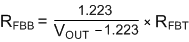
 Figure 7-1 FB Resistor Divider
| VOUT (V) | RFBB (kΩ) (1) | VOUT (V) | RFBB (kΩ) (1) | |
|---|---|---|---|---|
| 1.223 | open | 3.3 | 59.0 | |
| 1.5 | 442 | 5.0 | 32.4 | |
| 1.8 | 210 | 7.5 | 19.6 | |
| 2.0 | 158 | 10 | 14.0 | |
| 2.5 | 95.3 | 12 | 11.3 | |
| 3.0 | 68.1 | 15 | 8.87 |
Selecting an RFBT value of 100 kΩ is recommended for most applications. A larger RFBT consumes less DC current, which is mandatory if light-load efficiency, is critical. However, RFBT larger than 1 MΩ is not recommended as the feedback path becomes more susceptible to noise. High feedback resistance generally requires more careful layout of the feedback path. It is important to keep the feedback trace as short as possible while keeping the feedback trace away from the noisy area of the PCB. For more layout recommendations, see Section 10.