SNVSBF6B October 2019 – December 2020 TPSM265R1
PRODUCTION DATA
- 1 Features
- 2 Applications
- 3 Description
- 4 Revision History
- 5 Pin Configuration and Functions
-
6 Specifications
- 6.1 Absolute Maximum Ratings
- 6.2 ESD Ratings
- 6.3 Recommended Operating Conditions
- 6.4 Thermal Information
- 6.5 Electrical Characteristics
- 6.6 Typical Characteristics (VIN = 5 V)
- 6.7 Typical Characteristics (VIN = 12 V)
- 6.8 Typical Characteristics (VIN = 24 V)
- 6.9 Typical Characteristics (VIN = 48 V)
- 6.10 Typical Characteristics (VIN = 65 V)
-
7 Detailed Description
- 7.1 Overview
- 7.2 Functional Block Diagram
- 7.3
Feature Description
- 7.3.1 Adjustable Output Voltage (FB)
- 7.3.2 Input Capacitor Selection
- 7.3.3 Output Capacitor Selection
- 7.3.4 Precision Enable (EN), Undervoltage Lockout (UVLO), and Hysteresis (HYS)
- 7.3.5 PFM Operation
- 7.3.6 Power Good (PGOOD)
- 7.3.7 Configurable Soft Start (SS)
- 7.3.8 Overcurrent Protection (OCP)
- 7.3.9 Thermal Shutdown
- 7.4 Device Functional Modes
- 8 Applications and Implementation
- 9 Power Supply Recommendations
- 10Layout
- 11Device and Documentation Support
- 12Mechanical, Packaging, and Orderable Information
Package Options
Mechanical Data (Package|Pins)
- SIL|10
Thermal pad, mechanical data (Package|Pins)
Orderable Information
10.2.3 EMI
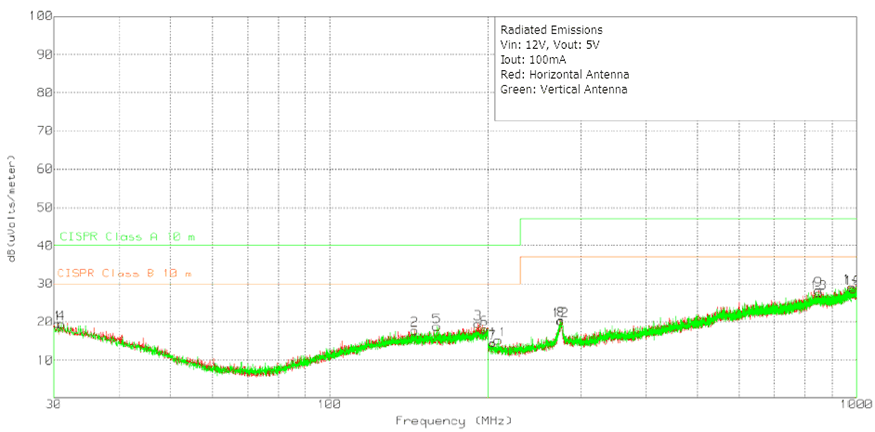
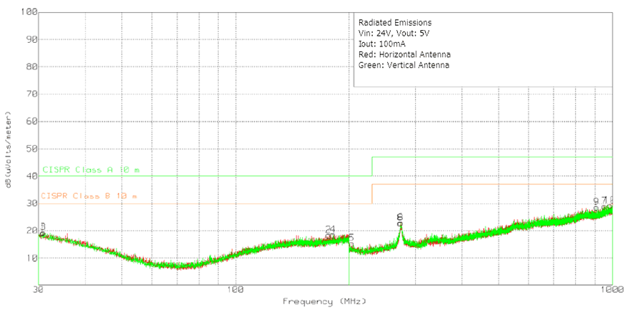
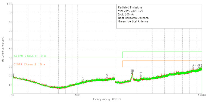
The TPSM265R1 is compliant with EN55011 radiated emissions. Figure 10-4, Figure 10-5, and Figure 10-6 show typical examples of radiated emission plots for the TPSM265R1. The graphs include the plots of the antenna in the horizontal and vertical positions.
EMI plots were measured using the standard TPSM265R1EVM with no input filter.
 Figure 10-4 Radiated Emissions 12-V Input, 5-V Output, 100-mA Load
 Figure 10-5 Radiated Emissions 24-V Input, 5-V Output, 100-mA Load
 Figure 10-6 Radiated Emissions 24-V Input, 12-V Output, 100-mA Load