SNVSCB1C December 2022 – February 2024 TPSM33615 , TPSM33625
PRODUCTION DATA
- 1
- 1 Features
- 2 Applications
- 3 Description
- 4 Device Comparison Table
- 5 Pin Configuration and Functions
- 6 Specifications
-
7 Detailed Description
- 7.1 Overview
- 7.2 Functional Block Diagram
- 7.3
Feature Description
- 7.3.1 Input Voltage Range
- 7.3.2 Output Voltage Selection
- 7.3.3 Input Capacitors
- 7.3.4 Output Capacitors
- 7.3.5 Enable, Start-Up, and Shutdown
- 7.3.6 External CLK SYNC (with MODE/SYNC)
- 7.3.7 Switching Frequency (RT)
- 7.3.8 Power-Good Output Operation
- 7.3.9 Internal LDO, VCC and VOUT/FB Input
- 7.3.10 Bootstrap Voltage and VBOOT-UVLO (BOOT Terminal)
- 7.3.11 Spread Spectrum
- 7.3.12 Soft Start and Recovery from Dropout
- 7.3.13 Overcurrent Protection (Hiccup Mode)
- 7.3.14 Thermal Shutdown
- 7.4 Device Functional Modes
-
8 Application and Implementation
- 8.1 Application Information
- 8.2
Typical Application
- 8.2.1 Design Requirements
- 8.2.2
Detailed Design Procedure
- 8.2.2.1 Custom Design With WEBENCH® Tools
- 8.2.2.2 Choosing the Switching Frequency
- 8.2.2.3 Setting the Output Voltage
- 8.2.2.4 Input Capacitor Selection
- 8.2.2.5 Output Capacitor Selection
- 8.2.2.6 VCC
- 8.2.2.7 CFF Selection
- 8.2.2.8 Power Good Signal
- 8.2.2.9 Maximum Ambient Temperature
- 8.2.2.10 Other Connections
- 8.2.3 Application Curves
- 8.3 Best Design Practices
- 8.4 Power Supply Recommendations
- 8.5 Layout
- 9 Device and Documentation Support
- 10Revision History
- 11Mechanical, Packaging, and Orderable Information
Package Options
Mechanical Data (Package|Pins)
- RDN|11
Thermal pad, mechanical data (Package|Pins)
Orderable Information
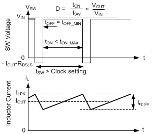
7.4.3.5 Dropout
Dropout operation is defined as any input-to-output voltage ratio that requires frequency to drop to achieve the required duty cycle. At a given clock frequency, duty cycle is limited by minimum off time. After this limit is reached as shown in Figure 7-18 if clock frequency was to be maintained, the output voltage can fall. Instead of allowing the output voltage to drop, the TPSM336x5 extends the high-side switch on time past the end of the clock cycle until the needed peak inductor current is achieved. The clock is allowed to start a new cycle after peak inductor current is achieved or after a pre-determined maximum on time, tON-MAX, of approximately 9 µs passes. As a result, after the needed duty cycle cannot be achieved at the selected clock frequency due to the existence of a minimum off time, frequency drops to maintain regulation. As shown in Figure 7-17, if input voltage is low enough so that output voltage cannot be regulated even with an on time of tON-MAX, output voltage drops to slightly below the input voltage by VDROP. For additional information on recovery from dropout, refer to Section 7.3.12.1.

