SNVSB77B December 2019 – September 2021 TPSM53603
PRODUCTION DATA
- 1 Features
- 2 Applications
- 3 Description
- 4 Revision History
- 5 Pin Configuration and Functions
- 6 Specifications
-
7 Detailed Description
- 7.1 Overview
- 7.2 Functional Block Diagram
- 7.3
Feature Description
- 7.3.1 Adjusting the Output Voltage
- 7.3.2 Switching Frequency
- 7.3.3 Input Capacitors
- 7.3.4 Output Capacitors
- 7.3.5 Output On/Off Enable (EN)
- 7.3.6 Programmable Undervoltage Lockout (UVLO)
- 7.3.7 Power Good (PGOOD)
- 7.3.8 Light Load Operation
- 7.3.9 Voltage Dropout
- 7.3.10 Overcurrent Protection (OCP)
- 7.3.11 Thermal Shutdown
- 7.4 Device Functional Modes
- 8 Application and Implementation
- 9 Power Supply Recommendations
- 10Layout
- 11Device and Documentation Support
- 12Mechanical, Packaging, and Orderable Information
Package Options
Mechanical Data (Package|Pins)
- RDA|15
Thermal pad, mechanical data (Package|Pins)
Orderable Information
3 Description
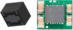
The TPSM53603 power module is a highly integrated 3-A power solution that combines a 36-V input, step-down, DC/DC converter with power MOSFETs, a shielded inductor, and passives in a thermally-enhanced QFN package. The 5-mm x 5.5-mm x 4-mm, 15-pin package uses Enhanced HotRod QFN technology for improved thermal performance, small footprint, and low EMI. The package footprint has all pins accessible from the perimeter and a single large thermal pad for simple layout and easy handling in manufacturing.
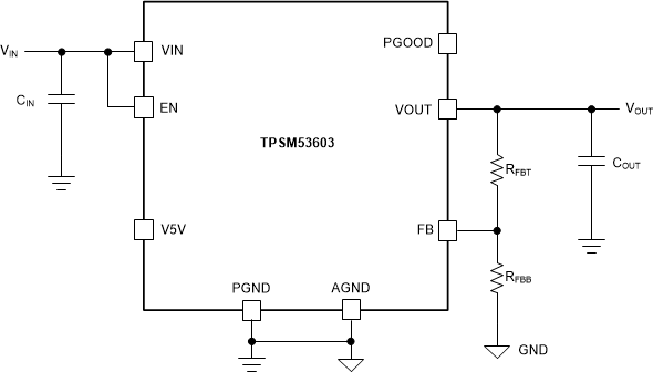
The total solution requires as few as four external components and eliminates the loop compensation and magnetics part selection from the design process. The full feature set includes power good, programmable UVLO, prebias start-up, overcurrent, and overtemperature protections, making the TPSM53603 an excellent device for powering a wide range of applications.
| DEVICE NUMBER (1) | PACKAGE | BODY SIZE (NOM) |
|---|---|---|
| TPSM53603 | B3QFN (15) | 5.0 mm × 5.5 mm |
 Enhanced
HotRod QFN and Typical Layout
 Simplified Schematic
 5
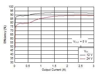
VOUT Efficiency