SNVSBC9C November 2019 – September 2021 TPSM53604
PRODUCTION DATA
- 1 Features
- 2 Applications
- 3 Description
- 4 Revision History
- 5 Pin Configuration and Functions
- 6 Specifications
-
7 Detailed Description
- 7.1 Overview
- 7.2 Functional Block Diagram
- 7.3
Feature Description
- 7.3.1 Adjusting the Output Voltage
- 7.3.2 Switching Frequency
- 7.3.3 Input Capacitors
- 7.3.4 Output Capacitors
- 7.3.5 Output On/Off Enable (EN)
- 7.3.6 Programmable Undervoltage Lockout (UVLO)
- 7.3.7 Power Good (PGOOD)
- 7.3.8 Light Load Operation
- 7.3.9 Voltage Dropout
- 7.3.10 Overcurrent Protection (OCP)
- 7.3.11 Thermal Shutdown
- 7.4 Device Functional Modes
- 8 Application and Implementation
- 9 Power Supply Recommendations
- 10Layout
- 11Device and Documentation Support
- 12Mechanical, Packaging, and Orderable Information
Package Options
Mechanical Data (Package|Pins)
- RDA|15
Thermal pad, mechanical data (Package|Pins)
Orderable Information
7.3.6 Programmable Undervoltage Lockout (UVLO)
The TPSM53604 implements internal UVLO circuitry on the VIN pin. The device is disabled when the VIN pin voltage falls below the internal VIN UVLO threshold. The internal VIN UVLO rising threshold is 3.55 V (typical) with a typical hysteresis of 500 mV.
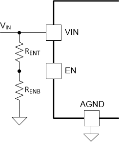
If an application requires a higher UVLO threshold, a resistor divider can be placed between VIN, the EN pin, and AGND as shown in Figure 7-5. The enable rising threshold (VEN-H) is 1.23 V (typ) with 100 mV (typ) hysteresis. Table 7-4 lists recommended resistor values for RENT and RENB to adjust the ULVO voltage.
To ensure proper start-up and reduce input current surges, TI recommends setting the UVLO threshold to approximately 80% to 85% of the minimum expected input voltage.
 Figure 7-5 Adjustable UVLO
| VIN UVLO (V) | 6.5 | 10 | 15 | 20 | 25 | 30 |
|---|---|---|---|---|---|---|
| RENT (kΩ) | 100 | 100 | 100 | 100 | 100 | 100 |
| RENB (kΩ) | 23.7 | 14.3 | 9.09 | 6.65 | 5.23 | 4.32 |