SLVSFI4B December   2020  – October 2021 TPSM5601R5H , TPSM5601R5HE

PRODUCTION DATA  

  1. Features
  2. Applications
  3. Description
  4. Revision History
  5. Device Comparison Table
  6. Pin Configuration and Functions
  7. Specifications
    1. 7.1 Absolute Maximum Ratings
    2. 7.2 ESD Ratings
    3. 7.3 Recommended Operating Conditions
    4. 7.4 Thermal Information
    5. 7.5 Electrical Characteristics
    6. 7.6 Typical Characteristics (VIN = 12 V)
    7. 7.7 Typical Characteristics (VIN = 24 V)
    8. 7.8 Typical Characteristics (VIN = 48 V)
    9. 7.9 Typical Characteristics (VIN = 60 V)
  8. Detailed Description
    1. 8.1 Overview
    2. 8.2 Functional Block Diagram
    3. 8.3 Feature Description
      1. 8.3.1 Adjustable Output Voltage (FB)
      2. 8.3.2 Minimum Input Capacitance
      3. 8.3.3 Minimum Output Capacitance
      4. 8.3.4 Precision Enable (EN), Undervoltage Lockout (UVLO), and Hysteresis (HYS)
      5. 8.3.5 Power Good (PGOOD)
      6. 8.3.6 Spread Spectrum Operation
      7. 8.3.7 Overcurrent Protection (OCP)
      8. 8.3.8 Thermal Shutdown
    4. 8.4 Device Functional Modes
      1. 8.4.1 Active Mode
      2. 8.4.2 Standby Mode
      3. 8.4.3 Shutdown Mode
  9. Applications and Implementation
    1. 9.1 Application Information
    2. 9.2 Typical Application
      1. 9.2.1 Design Requirements
      2. 9.2.2 Detailed Design Procedure
        1. 9.2.2.1 Custom Design With WEBENCH® Tools
        2. 9.2.2.2 Output Voltage Setpoint
        3. 9.2.2.3 Input Capacitors
        4. 9.2.2.4 Output Capacitor Selection
        5. 9.2.2.5 Power Good Signal
      3. 9.2.3 Application Curves
  10. 10Power Supply Recommendations
  11. 11Layout
    1. 11.1 Layout Guidelines
    2. 11.2 Layout Example
      1. 11.2.1 Theta JA versus PCB Area
      2. 11.2.2 Package Specifications
      3. 11.2.3 EMI
        1. 11.2.3.1 EMI Plots
  12. 12Device and Documentation Support
    1. 12.1 Device Support
      1. 12.1.1 Third-Party Products Disclaimer
      2. 12.1.2 Development Support
        1. 12.1.2.1 Custom Design With WEBENCH® Tools
    2. 12.2 Documentation Support
      1. 12.2.1 Related Documentation
    3. 12.3 Receiving Notification of Documentation Updates
    4. 12.4 Support Resources
    5. 12.5 Trademarks
    6. 12.6 Electrostatic Discharge Caution
    7. 12.7 Glossary
  13. 13Mechanical, Packaging, and Orderable Information

Package Options

Mechanical Data (Package|Pins)
Thermal pad, mechanical data (Package|Pins)
Orderable Information

Theta JA versus PCB Area

The amount of PCB copper as well as airflow effects the thermal performance of the device. Figure 11-5 shows the effects of copper area and airflow on the junction-to-ambient thermal resistance (RθJA) of the TPSM5601R5Hx. The junction-to-ambient thermal resistance versus PCB area is plotted for a 4-layer PCB.

To determine the required copper area for an application:

  1. Determine the maximum power dissipation of the device in the application by referencing the power dissipation graphs in the Typical Characteristics.
  2. Calculate the maximum θJA using Equation 3 and the maximum ambient temperature of the application.
    Equation 3. GUID-B3054877-0D10-4AEC-ABBC-939D6303BB83-low.gif
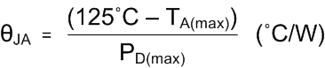
  3. Reference Figure 11-5 to determine the minimum required PCB area for the application conditions.

GUID-20210226-CA0I-7JXD-GK2B-ZBVCS0NQGVJL-low.gif Figure 11-5 θJA vs PCB Area