SLVSFI4B December 2020 – October 2021 TPSM5601R5H , TPSM5601R5HE
PRODUCTION DATA
- 1 Features
- 2 Applications
- 3 Description
- 4 Revision History
- 5 Device Comparison Table
- 6 Pin Configuration and Functions
-
7 Specifications
- 7.1 Absolute Maximum Ratings
- 7.2 ESD Ratings
- 7.3 Recommended Operating Conditions
- 7.4 Thermal Information
- 7.5 Electrical Characteristics
- 7.6 Typical Characteristics (VIN = 12 V)
- 7.7 Typical Characteristics (VIN = 24 V)
- 7.8 Typical Characteristics (VIN = 48 V)
- 7.9 Typical Characteristics (VIN = 60 V)
- 8 Detailed Description
- 9 Applications and Implementation
- 10Power Supply Recommendations
- 11Layout
- 12Device and Documentation Support
- 13Mechanical, Packaging, and Orderable Information
Package Options
Mechanical Data (Package|Pins)
- RDA|15
Thermal pad, mechanical data (Package|Pins)
Orderable Information
8.3.1 Adjustable Output Voltage (FB)
The TPSM5601R5Hx has an adjustable output voltage range of 1.0 V to 16 V. Setting the output voltage requires two resistors, RFBT and RFBB (see Figure 8-1). Connect RFBT between VOUT, at the regulation point, and the FB pin. Connect RFBB between the FB pin and AGND (pin 10). The recommended value of RFBT is 10 kΩ. The value for RFBB can be calculated using Equation 1.
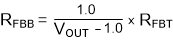
 Figure 8-1 FB Resistor Divider
| VOUT (V) | RFBB (kΩ) (1) | VOUT (V) | RFBB (kΩ) (1) | |
|---|---|---|---|---|
| 1.0 | open | 3.3 | 4.32 | |
| 1.2 | 49.9 | 5.0 | 2.49 | |
| 1.5 | 20.0 | 7.5 | 1.54 | |
| 1.8 | 12.4 | 10 | 1.10 | |
| 2.0 | 10.0 | 12 | 0.909 | |
| 2.5 | 6.65 | 15 | 0.715 | |
| 3.0 | 4.99 | 16 | 0.665 |
Selecting an RFBT value of 10 kΩ is recommended for most applications. A larger RFBT consumes less DC current, which is mandatory if light-load efficiency is critical. However, RFBT larger than 1 MΩ is not recommended as the feedback path becomes more susceptible to noise. High feedback resistance generally requires more careful layout of the feedback path. It is important to keep the feedback trace as short as possible while keeping the feedback trace away from the noisy area of the PCB. For more layout recommendations, see Section 11.