SLVSFS5A October 2021 – November 2021 TPSM63603
PRODUCTION DATA
- 1 Features
- 2 Applications
- 3 Description
- 4 Revision History
- 5 Pin Configuration and Functions
-
6 Specifications
- 6.1 Absolute Maximum Ratings
- 6.2 ESD Ratings
- 6.3 Recommended Operating Conditions
- 6.4 Thermal Information
- 6.5 Electrical Characteristics
- 6.6 System Characteristics
- 6.7 Typical Characteristics
- 6.8 Typical Characteristics: VIN = 12 V
- 6.9 Typical Characteristics: VIN = 24 V
- 6.10 Typical Characteristics: VIN = 36 V
-
7 Detailed Description
- 7.1 Overview
- 7.2 Functional Block Diagram
- 7.3
Feature Description
- 7.3.1 Input Voltage Range
- 7.3.2 Adjustable Output Voltage (FB)
- 7.3.3 Input Capacitors
- 7.3.4 Output Capacitors
- 7.3.5 Switching Frequency (RT)
- 7.3.6 Output ON/OFF Enable (EN/SYNC) and VIN UVLO
- 7.3.7 Frequency Synchronization (EN/SYNC)
- 7.3.8 Spread Spectrum
- 7.3.9 Power Good Monitor (PG)
- 7.3.10 Adjustable Switch-Node Slew Rate (RBOOT/CBOOT)
- 7.3.11 Internal LDO, VCC Output, and VLDOIN Input
- 7.3.12 Overcurrent Protection (OCP)
- 7.3.13 Thermal Shutdown
- 7.4 Device Functional Modes
-
8 Applications and Implementation
- 8.1 Application Information
- 8.2
Typical Applications
- 8.2.1 Design 1: 3-A Synchronous Buck Regulator for Industrial Applications
- 8.2.2 Design 2: Inverting Buck-Boost Regulator with a –5-V Output
- 9 Power Supply Recommendations
- 10Layout
- 11Device and Documentation Support
- 12Mechanical, Packaging, and Orderable Information
Package Options
Mechanical Data (Package|Pins)
- RDH|30
Thermal pad, mechanical data (Package|Pins)
Orderable Information
3 Description
The TPSM63603 synchronous buck power module is a highly integrated 36-V, 3-A DC/DC solution that combines power MOSFETs, a shielded inductor, and passives in an Enhanced HotRod™ QFN package. The module has pins for VIN and VOUT located at the corners of the package for optimized input and output capacitor layout placement. Four larger thermal pads beneath the module enable a simple layout and easy handling in manufacturing.
With an output voltage from 1 V to 16 V, the TPSM63603 is designed to quickly and easily implement a low-EMI design in a small PCB footprint. The total solution requires as few as four external components and eliminates the magnetics and compensation part selection from the design process.
Although designed for small size and simplicity in space-constrained applications, the TPSM63603 module offers many features for robust performance: precision enable with hysteresis for adjustable input-voltage UVLO, resistor-programmable switch node slew rate and spread spectrum option for improved EMI, integrated VCC, bootstrap and input capacitors for increased reliability and higher density, constant switching frequency over the full load current range, and a PGOOD indicator for sequencing, fault protection, and output voltage monitoring.
| PART NUMBER(1) | PACKAGE | BODY SIZE (NOM) |
|---|---|---|
| TPSM63603 | B0QFN (30) | 4.0 mm × 6.0 mm |
| TPSM63603S |
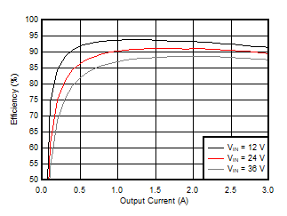
 Typical Efficiency, VOUT = 5 V,
FSW = 1 MHz