SLVSFS5A October   2021  – November 2021 TPSM63603

PRODUCTION DATA  

  1. Features
  2. Applications
  3. Description
  4. Revision History
  5. Pin Configuration and Functions
  6. Specifications
    1. 6.1  Absolute Maximum Ratings
    2. 6.2  ESD Ratings
    3. 6.3  Recommended Operating Conditions
    4. 6.4  Thermal Information
    5. 6.5  Electrical Characteristics
    6. 6.6  System Characteristics
    7. 6.7  Typical Characteristics
    8. 6.8  Typical Characteristics: VIN = 12 V
    9. 6.9  Typical Characteristics: VIN = 24 V
    10. 6.10 Typical Characteristics: VIN = 36 V
  7. Detailed Description
    1. 7.1 Overview
    2. 7.2 Functional Block Diagram
    3. 7.3 Feature Description
      1. 7.3.1  Input Voltage Range
      2. 7.3.2  Adjustable Output Voltage (FB)
      3. 7.3.3  Input Capacitors
      4. 7.3.4  Output Capacitors
      5. 7.3.5  Switching Frequency (RT)
      6. 7.3.6  Output ON/OFF Enable (EN/SYNC) and VIN UVLO
      7. 7.3.7  Frequency Synchronization (EN/SYNC)
      8. 7.3.8  Spread Spectrum
      9. 7.3.9  Power Good Monitor (PG)
      10. 7.3.10 Adjustable Switch-Node Slew Rate (RBOOT/CBOOT)
      11. 7.3.11 Internal LDO, VCC Output, and VLDOIN Input
      12. 7.3.12 Overcurrent Protection (OCP)
      13. 7.3.13 Thermal Shutdown
    4. 7.4 Device Functional Modes
      1. 7.4.1 Shutdown Mode
      2. 7.4.2 Standby Mode
      3. 7.4.3 Active Mode
  8. Applications and Implementation
    1. 8.1 Application Information
    2. 8.2 Typical Applications
      1. 8.2.1 Design 1: 3-A Synchronous Buck Regulator for Industrial Applications
        1. 8.2.1.1 Design Requirements
        2. 8.2.1.2 Detailed Design Procedure
          1. 8.2.1.2.1 Custom Design With WEBENCH® Tools
          2. 8.2.1.2.2 Output Voltage Setpoint
          3. 8.2.1.2.3 Switching Frequency Selection
          4. 8.2.1.2.4 Input Capacitor Selection
          5. 8.2.1.2.5 Output Capacitor Selection
          6. 8.2.1.2.6 Other Connections
        3. 8.2.1.3 Application Curves
      2. 8.2.2 Design 2: Inverting Buck-Boost Regulator with a –5-V Output
        1. 8.2.2.1 Design Requirements
        2. 8.2.2.2 Detailed Design Procedure
          1. 8.2.2.2.1 Output Voltage Setpoint
          2. 8.2.2.2.2 IBB Maximum Output Current
          3. 8.2.2.2.3 Switching Frequency Selection
          4. 8.2.2.2.4 Input Capacitor Selection
          5. 8.2.2.2.5 Output Capacitor Selection
          6. 8.2.2.2.6 Other Connections
        3. 8.2.2.3 Application Curves
        4. 8.2.2.4 EMI
          1. 8.2.2.4.1 EMI Plots
  9. Power Supply Recommendations
  10. 10Layout
    1. 10.1 Layout Guidelines
    2. 10.2 Layout Example
      1. 10.2.1 Package Specifications
  11. 11Device and Documentation Support
    1. 11.1 Device Support
      1. 11.1.1 Third-Party Products Disclaimer
      2. 11.1.2 Development Support
        1. 11.1.2.1 Custom Design With WEBENCH® Tools
    2. 11.2 Documentation Support
      1. 11.2.1 Related Documentation
    3. 11.3 Receiving Notification of Documentation Updates
    4. 11.4 Support Resources
    5. 11.5 Trademarks
    6. 11.6 Electrostatic Discharge Caution
    7. 11.7 Glossary
  12. 12Mechanical, Packaging, and Orderable Information

Package Options

Mechanical Data (Package|Pins)
Thermal pad, mechanical data (Package|Pins)
Orderable Information

Typical Characteristics: VIN = 12 V

Refer to Section 8.2 for circuit designs.
GUID-20210318-CA0I-FP2M-SJ4P-N08HQC5SDBH2-low.gif
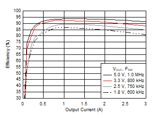
VLDOIN = VOUT
Figure 6-7 Efficiency
GUID-20210318-CA0I-KBH0-C3Q1-JNLVJFD8BVGQ-low.gif
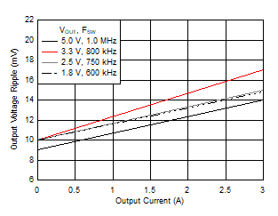
COUT = 2 × 47-µF ceramic, 25-V, 1206 case size
Figure 6-9 Output Voltage Ripple
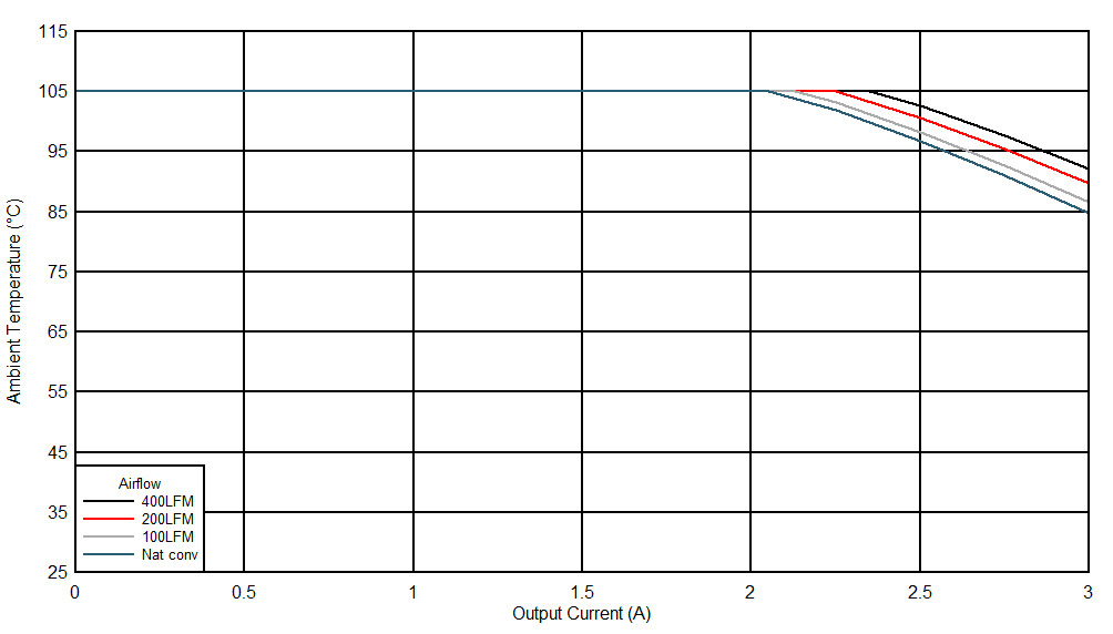
GUID-20210318-CA0I-CBGT-PPH9-RTBR7J0HGNHQ-low.gif
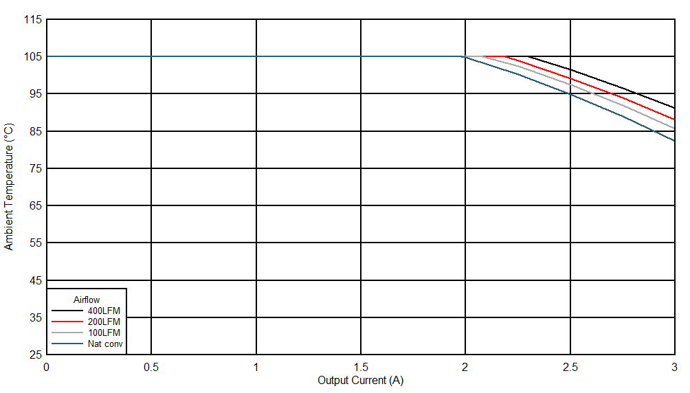
Device soldered to a 64-mm × 83-mm, 4-layer PCB
Figure 6-11 Safe Operating Area
VOUT = 3.3 V, FSW = 800 kHz
GUID-20210318-CA0I-ZDV6-QSC2-9ZSVRDGC7CBF-low.gif
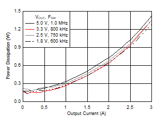
VLDOIN = VOUT
Figure 6-8 Power Dissipation
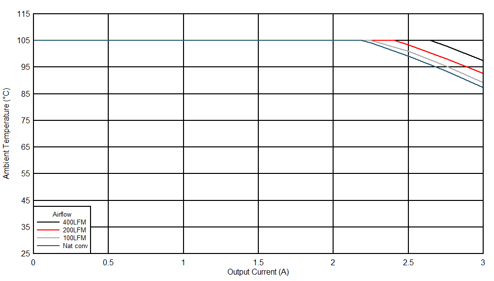
GUID-20210323-CA0I-7RPV-B1NK-GPMTNPPKRV9K-low.gif
Device soldered to a 64-mm × 83-mm, 4-layer PCB
Figure 6-10 Safe Operating Area
VOUT = 1.8 V, FSW = 600 kHz
GUID-20210323-CA0I-7R3B-CGLN-DPB0JRHCKQFZ-low.gif
Device soldered to a 64-mm × 83-mm, 4-layer PCB
Figure 6-12 Safe Operating Area
VOUT = 5.0 V, FSW = 1 MHz