SLVSGL3 April 2022 TPSM63603E
PRODUCTION DATA
- 1 Features
- 2 Applications
- 3 Description
- 4 Revision History
- 5 Device Comparison Table
- 6 Pin Configuration and Functions
-
7 Specifications
- 7.1 Absolute Maximum Ratings
- 7.2 ESD Ratings
- 7.3 Recommended Operating Conditions
- 7.4 Thermal Information
- 7.5 Electrical Characteristics
- 7.6 System Characteristics
- 7.7 Typical Characteristics
- 7.8 Typical Characteristics — VIN = 12 V
- 7.9 Typical Characteristics — VIN = 24 V
- 7.10 Typical Characteristics — VIN = 36 V
-
8 Detailed Description
- 8.1 Overview
- 8.2 Functional Block Diagram
- 8.3
Feature Description
- 8.3.1 Input Voltage Range
- 8.3.2 Adjustable Output Voltage (FB)
- 8.3.3 Input Capacitors
- 8.3.4 Output Capacitors
- 8.3.5 Switching Frequency (RT)
- 8.3.6 Output ON and OFF Enable (EN/SYNC) and VIN UVLO
- 8.3.7 Frequency Synchronization (EN/SYNC)
- 8.3.8 Spread Spectrum
- 8.3.9 Power-Good Monitor (PG)
- 8.3.10 Adjustable Switch-Node Slew Rate (RBOOT and CBOOT)
- 8.3.11 Internal LDO, VCC Output, and VLDOIN Input
- 8.3.12 Overcurrent Protection (OCP)
- 8.3.13 Thermal Shutdown
- 8.4 Device Functional Modes
-
9 Applications and Implementation
- 9.1 Application Information
- 9.2 Typical Applications
- 10Power Supply Recommendations
- 11Layout
- 12Device and Documentation Support
- 13Mechanical, Packaging, and Orderable Information
Package Options
Mechanical Data (Package|Pins)
- RDH|30
Thermal pad, mechanical data (Package|Pins)
Orderable Information
8.3.7 Frequency Synchronization (EN/SYNC)
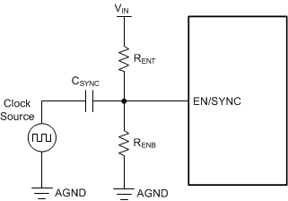
The TPSM63603E can be synchronized to an external clock using the EN/SYNC pin. The synchronization frequency range is 200 kHz to 2.2 MHz. The internal oscillator can be synchronized by AC coupling a positive clock edge into the EN/SYNC pin, as shown in Figure 8-4. It is recommended to keep the parallel combination value of RENT and RENB in the 100-kΩ range. RENT is required for synchronization, but RENB can be left open. The external clock must be off before start-up to allow proper start-up sequencing. After a valid synchronization signal is applied for 2048 cycles, the clock frequency changes to that of the applied signal.
 Figure 8-4 Typical Synchronization Using
the EN/SYNC Pin
Figure 8-4 Typical Synchronization Using
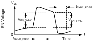
the EN/SYNC PinReferring to Figure 8-5, the AC-coupled voltage edge at the EN/SYNC pin must exceed the SYNC amplitude threshold, VEN_SYNC, of 2.4 V to trip the internal synchronization pulse detector. In addition, the minimum EN/SYNC rising pulse and falling pulse durations must be longer than the SYNC signal hold time, tSYNC_EDGE, of 100 ns and shorter than the minimum blanking time, tB. A 3.3-V or higher amplitude pulse signal coupled through a 1-nF capacitor, CSYNC, is suggested.
 Figure 8-5 Typical SYNC Waveform