SLVSDT1C July   2017  – June 2020 TPSM82480

PRODUCTION DATA.  

  1. Features
  2. Applications
  3. Description
    1.     Device Images
      1.      Typical Application space
      2.      Efficiency vs Output Current space space
  4. Revision History
  5. Pin Configuration and Functions
    1.     Pin Functions
  6. Specifications
    1. 6.1 Absolute Maximum Ratings
    2. 6.2 ESD Ratings
    3. 6.3 Recommended Operating Conditions
    4. 6.4 Thermal Information
    5. 6.5 Electrical Characteristics
    6. 6.6 Typical Characteristics
  7. Detailed Description
    1. 7.1 Overview
    2. 7.2 Functional Block Diagram
    3. 7.3 Feature Description
      1. 7.3.1  Enable and Shutdown (EN)
      2. 7.3.2  Soft-Start (SS), Pre-biased Output
      3. 7.3.3  Tracking (TR)
      4. 7.3.4  Output Voltage Select (VSEL)
      5. 7.3.5  Forced PWM (MODE)
      6. 7.3.6  Power Good (PG)
      7. 7.3.7  Thermal Good (TG)
      8. 7.3.8  Active Output Discharge
      9. 7.3.9  Undervoltage Lockout (UVLO)
      10. 7.3.10 Thermal Shutdown
    4. 7.4 Device Functional Modes
      1. 7.4.1 Pulse Width Modulation (PWM) Operation
      2. 7.4.2 Power Save Mode (PSM) Operation
      3. 7.4.3 Minimum Duty Cycle and 100% Mode Operation
      4. 7.4.4 Phase Shifted Operation
      5. 7.4.5 Phase Add/Shed and Current Balancing
      6. 7.4.6 Current Limit and Short Circuit Protection
  8. Application and Implementation
    1. 8.1 Application Information
    2. 8.2 Typical Application
      1. 8.2.1 Design Requirements
      2. 8.2.2 Detailed Design Procedure
        1. 8.2.2.1 Setting the Output Voltage
        2. 8.2.2.2 Setting VOUT2 Using the VSEL Feature
        3. 8.2.2.3 Feedforward Capacitance
        4. 8.2.2.4 Output Capacitor Selection
        5. 8.2.2.5 Input Capacitor Selection
        6. 8.2.2.6 Soft-Start Capacitor Selection
        7. 8.2.2.7 Tracking
        8. 8.2.2.8 Thermal Good
      3. 8.2.3 Application Curves
    3. 8.3 System Examples
  9. Power Supply Recommendations
  10. 10Layout
    1. 10.1 Layout Guidelines
    2. 10.2 Layout Example
  11. 11Device and Documentation Support
    1. 11.1 Documentation Support
      1. 11.1.1 Related Documentation
    2. 11.2 Receiving Notification of Documentation Updates
    3. 11.3 Community Resources
    4. 11.4 Trademarks
    5. 11.5 Electrostatic Discharge Caution
    6. 11.6 Glossary
  12. 12Mechanical, Packaging, and Orderable Information
    1. 12.1 Tape and Reel Information

Package Options

Mechanical Data (Package|Pins)
Thermal pad, mechanical data (Package|Pins)
Orderable Information

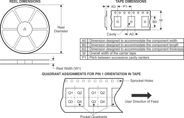
Tape and Reel Information

TPSM82480 Tape_and_Reel_Dims.gif
Device Package
Type
Package Drawing Pins SPQ Reel
Diameter (mm)
Reel
Width W1 (mm)
A0
(mm)
B0
(mm)
K0
(mm)
P1
(mm)
W
(mm)
Pin1
Quadrant
TPSM82480MOPR QFM MOP 24 3000 330.0 16.0 3.85 8.15 1.7 8.0 16.0 Q2
TPSM82480MOPT QFM MOP 24 250 180.0 16.0 3.85 8.15 1.7 8.0 16.0 Q2

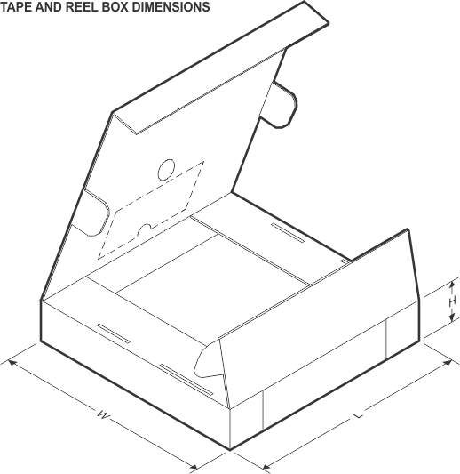
TPSM82480 Tape_and_Reel_Box_Dims.gif

Device Package Type Package Drawing Pins SPQ Length (mm) Width (mm) Height (mm)
TPSM82480MOPR QFM MOP 24 3000 383.0 353.0 58.0
TPSM82480MOPT QFM MOP 24 250 223.0 194.0 35.0