SLUSEY7 December   2022 TPSM82816

PRODUCTION DATA  

  1. Features
  2. Applications
  3. Description
  4. Revision History
  5. Device Comparison Table
  6. Pin Configuration and Functions
  7. Specifications
    1. 7.1 Absolute Maximum Ratings
    2. 7.2 ESD Ratings
    3. 7.3 Recommended Operating Conditions
    4. 7.4 Thermal Information
    5. 7.5 Electrical Characteristics
    6. 7.6 Typical Characteristics
  8. Detailed Description
    1. 8.1 Overview
    2. 8.2 Functional Block Diagram
    3. 8.3 Feature Description
      1. 8.3.1 Precise Enable (EN)
      2. 8.3.2 Output Discharge
      3. 8.3.3 COMP/FSET
      4. 8.3.4 MODE/SYNC
      5. 8.3.5 Spread Spectrum Clocking (SSC)
      6. 8.3.6 Undervoltage Lockout (UVLO)
      7. 8.3.7 Power-Good Output (PG)
      8. 8.3.8 Thermal Shutdown
    4. 8.4 Device Functional Modes
      1. 8.4.1 Pulse Width Modulation (PWM) Operation
      2. 8.4.2 Power Save Mode Operation (PSM)
      3. 8.4.3 100% Duty-Cycle Operation
      4. 8.4.4 Current Limit and Short-Circuit Protection
      5. 8.4.5 Soft Start / Tracking (SS/TR)
  9. Application and Implementation
    1. 9.1 Application Information
    2. 9.2 Typical Application
      1. 9.2.1 Design Requirements
      2. 9.2.2 Detailed Design Procedure
        1. 9.2.2.1 Setting the Output Voltage
        2. 9.2.2.2 Feedforward Capacitor
        3. 9.2.2.3 Input Capacitor
        4. 9.2.2.4 Output Capacitor
        5. 9.2.2.5 Application Curves
    3. 9.3 System Examples
      1. 9.3.1 Voltage Tracking
      2. 9.3.2 Synchronizing to an External Clock
    4. 9.4 Power Supply Recommendations
    5. 9.5 Layout
      1. 9.5.1 Layout Guidelines
      2. 9.5.2 Layout Example
        1. 9.5.2.1 Thermal Consideration
  10. 10Device and Documentation Support
    1. 10.1 Device Support
      1. 10.1.1 Third-Party Products Disclaimer
    2. 10.2 Documentation Support
      1. 10.2.1 Related Documentation
    3. 10.3 Receiving Notification of Documentation Updates
    4. 10.4 Support Resources
    5. 10.5 Trademarks
    6. 10.6 Electrostatic Discharge Caution
    7. 10.7 Glossary
  11. 11Mechanical, Packaging, and Orderable Information

Package Options

Refer to the PDF data sheet for device specific package drawings

Mechanical Data (Package|Pins)
  • SIE|14
Thermal pad, mechanical data (Package|Pins)
Orderable Information

Synchronizing to an External Clock

The TPSM82816 can be synchronized by applying a clock on the MODE/SYNC pin. There is no need for any additional circuitry as long as the input signal meets the requirements given in the electrical specifications. See Figure 9-25. The clock can be applied, changed, and removed during operation. The value of the RCF resistor is recommended to be chosen such that the internally defined frequency and the externally-applied frequency are close to each other to have a fast settling time to the external clock. Synchronizing to a clock is not possible if the COMP/FSET pin is connected to Vin or GND. Figure 9-26 and Figure 9-27 show the external clock being applied and removed. When an external clock is applied, the device operates in PWM mode.
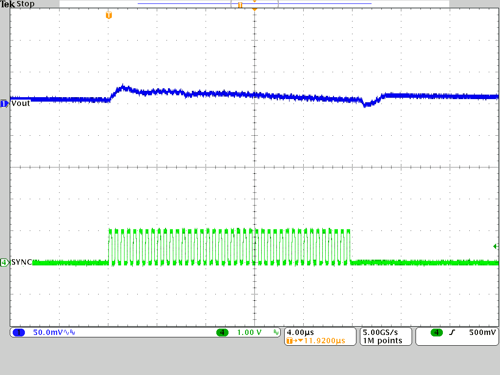
Figure 9-25 Frequency Synchronization
GUID-20221024-SS0I-6TTB-ZP58-KSHRHG5M6VGB-low.png
VIN = 5 VRCF = 10 kΩIOUT = 0.01 A
VOUT = 1.8 VfEXT = 2.0 MHz
Figure 9-26 Applying and Removing the Synchronization Signal (PSM)
GUID-20221024-SS0I-GTCX-9ZBJ-CSTBKG1VZWNH-low.png
VIN = 5 VRCF = 10 kΩIOUT = 1 A
VOUT = 1.8 VfEXT = 2.0 MHz
Figure 9-27 Applying and Removing the Synchronization Signal (FPWM)