SLVSEP0F August   2019  – November 2021 TPSM82821 , TPSM82821A , TPSM82822 , TPSM82822A , TPSM82823 , TPSM82823A

PRODUCTION DATA  

  1. Features
  2. Applications
  3. Description
  4. Revision History
  5. Device Comparison Table
  6. Pin Configuration and Functions
  7. Specifications
    1. 7.1 Absolute Maximum Ratings
    2. 7.2 ESD Ratings
    3. 7.3 Recommended Operating Conditions
    4. 7.4 Thermal Information
    5. 7.5 Electrical Characteristics
    6. 7.6 Typical Characteristics
  8. Detailed Description
    1. 8.1 Overview
    2. 8.2 Functional Block Diagram
    3. 8.3 Feature Description
      1. 8.3.1 PWM and PSM Operation
      2. 8.3.2 Low Dropout Operation (100% Duty Cycle)
      3. 8.3.3 Soft Start-up
      4. 8.3.4 Switch Current Limit and Hiccup Short Circuit Protection
      5. 8.3.5 Undervoltage Lockout
      6. 8.3.6 Thermal Shutdown
    4. 8.4 Device Functional Modes
      1. 8.4.1 Enable and Disable
      2. 8.4.2 Output Discharge
      3. 8.4.3 Power Good Output
  9. Application and Implementation
    1. 9.1 Application Information
    2. 9.2 Typical Applications
      1. 9.2.1 1.8-V Output Application
        1. 9.2.1.1 Design Requirements
        2. 9.2.1.2 Detailed Design Procedure
          1. 9.2.1.2.1 Setting the Output Voltage
          2. 9.2.1.2.2 Feedforward capacitor
          3. 9.2.1.2.3 Input and Output Capacitor Selection
        3. 9.2.1.3 Application Performance Curves
          1. 9.2.1.3.1 TPSM82821 Performance Curves
          2. 9.2.1.3.2 TPSM82821A Performance Curves
          3. 9.2.1.3.3 TPSM82822 Performance Curves
          4. 9.2.1.3.4 TPSM82822A Performance Curves
          5. 9.2.1.3.5 TPSM82823 Performance Curves
          6. 9.2.1.3.6 TPSM82823A Performance Curves
  10. 10Power Supply Recommendations
  11. 11Layout
    1. 11.1 Layout Guidelines
    2. 11.2 Layout Example
      1. 11.2.1 Thermal Consideration
  12. 12Device and Documentation Support
    1. 12.1 Device Support
      1. 12.1.1 Third-Party Products Disclaimer
      2. 12.1.2 Development Support
        1. 12.1.2.1 Models and Simulators
    2. 12.2 Documentation Support
      1. 12.2.1 Related Documentation
    3. 12.3 Receiving Notification of Documentation Updates
    4. 12.4 Trademarks
    5. 12.5 Electrostatic Discharge Caution
    6. 12.6 Glossary

Package Options

Refer to the PDF data sheet for device specific package drawings

Mechanical Data (Package|Pins)
  • SIL|10
Thermal pad, mechanical data (Package|Pins)
Orderable Information

Pin Configuration and Functions

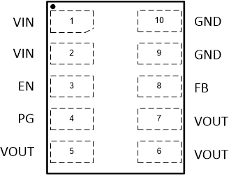
GUID-F18ECDF6-EF4F-4217-919C-3DE02B466A3F-low.gifFigure 6-1 µSiL Package(Top View)
Table 6-1 Pin Functions
PINI/ODESCRIPTION
NAMENO.
EN3IDevice enable pin. To enable the device, this pin needs to be pulled high. Pulling this pin low disables the device. Do not leave floating.
FB8IFeedback pin. This pin must be connected to the center of the output voltage resistor divider. For the fixed output voltage devices, connect this pin directly to the output voltage.
GND9, 10PWRGround pin
PG4OPower-good open-drain output pin with window comparator. The pullup resistor can be connected to voltages up to 5.5 V. If unused, leave it floating.
VIN1, 2PWRInput voltage pin
VOUT5, 6, 7PWROutput voltage pin