SLUSEO6B may 2023 – july 2023 TPSM843B22
PRODUCTION DATA
- 1
- 1 Features
- 2 Applications
- 3 Description
- 4 Revision History
- 5 Pin Configuration and Functions
- 6 Specifications
-
7 Detailed Description
- 7.1 Overview
- 7.2 Functional Block Diagram
- 7.3
Feature Description
- 7.3.1 VIN Pins and VIN UVLO
- 7.3.2 Internal Bypassing (BP5)
- 7.3.3 Enable and Adjustable UVLO
- 7.3.4 Switching Frequency Selection
- 7.3.5 Switching Frequency Synchronization to an External Clock
- 7.3.6 Remote Sense Amplifier and Adjusting the Output Voltage
- 7.3.7 Loop Compensation Guidelines
- 7.3.8 Soft Start and Prebiased Output Start-up
- 7.3.9 MSEL Pin
- 7.3.10 Power Good (PG)
- 7.3.11 Output Overload Protection
- 7.3.12 Output Overvoltage and Undervoltage Protection
- 7.3.13 Overtemperature Protection
- 7.3.14 Output Voltage Discharge
- 7.4 Device Functional Modes
-
8 Application and Implementation
- 8.1 Application Information
- 8.2
Typical Applications
- 8.2.1
1.0-V Output, 1-MHz Application
- 8.2.1.1 Design Requirements
- 8.2.1.2
Detailed Design Procedure
- 8.2.1.2.1 Switching Frequency
- 8.2.1.2.2 Output Inductor Selection
- 8.2.1.2.3 Output Capacitor
- 8.2.1.2.4 Input Capacitor
- 8.2.1.2.5 Adjustable Undervoltage Lockout
- 8.2.1.2.6 Output Voltage Resistors Selection
- 8.2.1.2.7 Bootstrap Capacitor Selection
- 8.2.1.2.8 BP5 Capacitor Selection
- 8.2.1.2.9 PG Pullup Resistor
- 8.2.1.2.10 Current Limit Selection
- 8.2.1.2.11 Soft-Start Time Selection
- 8.2.1.2.12 Ramp Selection and Control Loop Stability
- 8.2.1.2.13 MSEL Pin
- 8.2.1.3 Application Curves
- 8.2.1
1.0-V Output, 1-MHz Application
- 8.3 Power Supply Recommendations
- 8.4 Layout
- 9 Device and Documentation Support
- 10Mechanical, Packaging, and Orderable Information
Package Options
Mechanical Data (Package|Pins)
- RDG|25
Thermal pad, mechanical data (Package|Pins)
Orderable Information
8.2.1.2.3 Output Capacitor
There are two primary considerations for selecting the value of the output capacitor. The output voltage ripple and how the regulator responds to a large change in load current. The output capacitance must be selected based on the more stringent of these criteria.
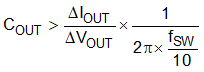
The desired response to a large change in the load current is the first criteria and is typically the most stringent. A regulator does not respond immediately to a large, fast increase or decrease in load current. The output capacitor supplies or absorbs charge until the regulator responds to the load step. The control loop must sense the change in the output voltage then adjust the peak switch current in response to the change in load. The minimum output capacitance is selected based on an estimate of the loop bandwidth. Typically, the loop bandwidth is near fSW / 10. Equation 16 estimates the minimum output capacitance necessary.
For this example, the transient load response is specified as a 5% change in VOUT for a load step of 10 A. Therefore, ΔIOUT is 10 A and ΔVOUT is 50 mV. Using this target gives a minimum capacitance of 318 μF. This value does not take the ESR of the output capacitor into account in the output voltage change. For ceramic capacitors, the effect of the ESR can be small enough to be ignored. Aluminum electrolytic and tantalum capacitors have higher ESR that must be considered for load step response.
where
- ΔIOUT is the change in output current.
- ΔVOUT is the allowable change in the output voltage.
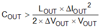
In addition to the loop bandwidth, the inductor current slew rate limiting how quickly the regulator responds to the load step is possible. For low duty cycle applications, the time it takes for the inductor current to ramp down after a load step down can be the limiting factor. Equation 17 estimates the minimum output capacitance necessary to limit the change in the output voltage after a load step down. Using the 330-nH inductance selected gives a minimum capacitance of 138 µF.
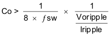
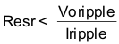
Equation 18 calculates the minimum output capacitance needed to meet the output voltage ripple specification. In this case, the target maximum steady state output voltage ripple is 10 mV. Under this requirement, Equation 18 yields 34 µF.
where
- ΔIOUT is the change in output current.
- ΔVOUT is the allowable change in the output voltage.
- fSW is the regulators switching frequency.
- VORIPPLE is the maximum allowable steady state output voltage ripple.
- IRIPPLE is the inductor ripple current.
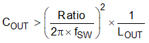
Lastly, if an application does not have a strict load transient response or output ripple requirement, a minimum amount of capacitance is still required to ensure the control loop is stable with the lowest gain ramp setting on the MSEL pin. Equation 19 estimates the minimum capacitance needed for loop stability. Equation 19 sets the minimum amount of capacitance by keeping the LC frequency relative to the switching frequency at a minimum value. See Figure 8-3 for the limit versus output voltage with the lowest gain ramp setting of 1 pF. With a 1-V output, the minimum ratio is 35 and with this ratio, Equation 19 gives a minimum capacitance of 94 µF.
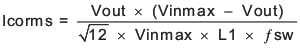
Equation 20 calculates the maximum combined ESR the output capacitors can have to meet the output voltage ripple specification and this shows the ESR must be less than 6 mΩ. In this case, ceramic capacitors are used and the combined ESR of the ceramic capacitors in parallel is much less than is needed to meet the ripple. Capacitors also have limits to the amount of ripple current they can handle without producing excess heat and failing. An output capacitor that can support the inductor ripple current must be specified. The capacitor data sheet specifies the RMS value of the maximum ripple current. Equation 21 can be used to calculate the RMS ripple current the output capacitor must support. For this application, Equation 21 yields 0.8 A and ceramic capacitors typically have a ripple current rating much higher than this.
Select X5R and X7R ceramic dielectrics or equivalent for power regulator capacitors because they have a high capacitance to volume ratio and are fairly stable over temperature. The output capacitor must also be selected with the DC bias and AC voltage derating taken into account. The derated capacitance value of a ceramic capacitor due to DC voltage bias and AC RMS voltage is usually found on the capacitor manufacturer's website. For this application example, four 100-µF, 10-V, X5R, 1210 ceramic capacitors each with 3 mΩ of ESR are used. With the four parallel capacitors, the estimated effective output capacitance after derating using the capacitor manufacturer's website is 380 µF. There is about -5% DC bias derating at 1 V. This design was able to use less than the calculated minimum because the loop crossover frequency was above the fSW / 10 estimate as shown in Figure 8-8.