SLUSEO6B may 2023 – july 2023 TPSM843B22
PRODUCTION DATA
- 1
- 1 Features
- 2 Applications
- 3 Description
- 4 Revision History
- 5 Pin Configuration and Functions
- 6 Specifications
-
7 Detailed Description
- 7.1 Overview
- 7.2 Functional Block Diagram
- 7.3
Feature Description
- 7.3.1 VIN Pins and VIN UVLO
- 7.3.2 Internal Bypassing (BP5)
- 7.3.3 Enable and Adjustable UVLO
- 7.3.4 Switching Frequency Selection
- 7.3.5 Switching Frequency Synchronization to an External Clock
- 7.3.6 Remote Sense Amplifier and Adjusting the Output Voltage
- 7.3.7 Loop Compensation Guidelines
- 7.3.8 Soft Start and Prebiased Output Start-up
- 7.3.9 MSEL Pin
- 7.3.10 Power Good (PG)
- 7.3.11 Output Overload Protection
- 7.3.12 Output Overvoltage and Undervoltage Protection
- 7.3.13 Overtemperature Protection
- 7.3.14 Output Voltage Discharge
- 7.4 Device Functional Modes
-
8 Application and Implementation
- 8.1 Application Information
- 8.2
Typical Applications
- 8.2.1
1.0-V Output, 1-MHz Application
- 8.2.1.1 Design Requirements
- 8.2.1.2
Detailed Design Procedure
- 8.2.1.2.1 Switching Frequency
- 8.2.1.2.2 Output Inductor Selection
- 8.2.1.2.3 Output Capacitor
- 8.2.1.2.4 Input Capacitor
- 8.2.1.2.5 Adjustable Undervoltage Lockout
- 8.2.1.2.6 Output Voltage Resistors Selection
- 8.2.1.2.7 Bootstrap Capacitor Selection
- 8.2.1.2.8 BP5 Capacitor Selection
- 8.2.1.2.9 PG Pullup Resistor
- 8.2.1.2.10 Current Limit Selection
- 8.2.1.2.11 Soft-Start Time Selection
- 8.2.1.2.12 Ramp Selection and Control Loop Stability
- 8.2.1.2.13 MSEL Pin
- 8.2.1.3 Application Curves
- 8.2.1
1.0-V Output, 1-MHz Application
- 8.3 Power Supply Recommendations
- 8.4 Layout
- 9 Device and Documentation Support
- 10Mechanical, Packaging, and Orderable Information
Package Options
Mechanical Data (Package|Pins)
- RDG|25
Thermal pad, mechanical data (Package|Pins)
Orderable Information
7.3.3 Enable and Adjustable UVLO
The EN pin provides means for on and off control of the device. After the EN pin voltage exceeds its threshold voltage, the device begins a start-up sequence. If the EN pin voltage is pulled below the threshold voltage, the regulator stops switching and enters a low operating current state. The EN pin has an internal pullup current source, IP, allowing the pin to be floated to enable the device by default. Ensure that leakage current of any circuitry connected to the EN pin does not exceed the minimum EN pullup current, otherwise the device can not be able to start. If an application requires digital control of the ENABLE function, an open-drain or open-collector output logic can be interfaced with the pin.
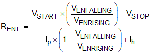
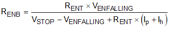
Alternatively, an external resistor divider can be added from VIN to the EN pin for adjustable UVLO as shown in Figure 7-1. The EN pin pullup hysteresis current, Ih, is used to control the voltage hysteresis for the UVLO function by increasing the pin sourcing current after the EN pin crosses the enable threshold. The UVLO thresholds can be calculated using Equation 1 and Equation 2. When using the adjustable UVLO function, 500 mV or greater hysteresis is recommended. For applications with very slow input voltage slew rate, a capacitor can be placed from the EN pin to ground to filter any noise on the input voltage.
 Figure 7-1 Adjustable UVLO Using EN