SLUSEO6B may 2023 – july 2023 TPSM843B22
PRODUCTION DATA
- 1
- 1 Features
- 2 Applications
- 3 Description
- 4 Revision History
- 5 Pin Configuration and Functions
- 6 Specifications
-
7 Detailed Description
- 7.1 Overview
- 7.2 Functional Block Diagram
- 7.3
Feature Description
- 7.3.1 VIN Pins and VIN UVLO
- 7.3.2 Internal Bypassing (BP5)
- 7.3.3 Enable and Adjustable UVLO
- 7.3.4 Switching Frequency Selection
- 7.3.5 Switching Frequency Synchronization to an External Clock
- 7.3.6 Remote Sense Amplifier and Adjusting the Output Voltage
- 7.3.7 Loop Compensation Guidelines
- 7.3.8 Soft Start and Prebiased Output Start-up
- 7.3.9 MSEL Pin
- 7.3.10 Power Good (PG)
- 7.3.11 Output Overload Protection
- 7.3.12 Output Overvoltage and Undervoltage Protection
- 7.3.13 Overtemperature Protection
- 7.3.14 Output Voltage Discharge
- 7.4 Device Functional Modes
-
8 Application and Implementation
- 8.1 Application Information
- 8.2
Typical Applications
- 8.2.1
1.0-V Output, 1-MHz Application
- 8.2.1.1 Design Requirements
- 8.2.1.2
Detailed Design Procedure
- 8.2.1.2.1 Switching Frequency
- 8.2.1.2.2 Output Inductor Selection
- 8.2.1.2.3 Output Capacitor
- 8.2.1.2.4 Input Capacitor
- 8.2.1.2.5 Adjustable Undervoltage Lockout
- 8.2.1.2.6 Output Voltage Resistors Selection
- 8.2.1.2.7 Bootstrap Capacitor Selection
- 8.2.1.2.8 BP5 Capacitor Selection
- 8.2.1.2.9 PG Pullup Resistor
- 8.2.1.2.10 Current Limit Selection
- 8.2.1.2.11 Soft-Start Time Selection
- 8.2.1.2.12 Ramp Selection and Control Loop Stability
- 8.2.1.2.13 MSEL Pin
- 8.2.1.3 Application Curves
- 8.2.1
1.0-V Output, 1-MHz Application
- 8.3 Power Supply Recommendations
- 8.4 Layout
- 9 Device and Documentation Support
- 10Mechanical, Packaging, and Orderable Information
Package Options
Mechanical Data (Package|Pins)
- RDG|25
Thermal pad, mechanical data (Package|Pins)
Orderable Information
8.2.1.2.1 Switching Frequency
The first step is to decide on a switching frequency. The TPSM843B22 can operate at five different frequencies from 500 kHz to 2.2 MHz. fSW is set by the resistor value from the FSEL pin to ground. Typically, the highest switching frequency possible is desired because it produces the smallest solution size. A high switching frequency allows for smaller inductors and output capacitors compared to a power supply that switches at a lower frequency. The main tradeoff made with selecting a higher switching frequency is extra switching power loss, which hurts the efficiency of the regulator.
The maximum switching frequency for a given application can be limited by the minimum on time of the regulator and the maximum fSW can be estimated with Equation 15. Using the maximum minimum on time of 40 ns and 18.0-V maximum input voltage for this application, the maximum switching frequency is 1389 kHz. The selected switching frequency must also consider the tolerance of the switching frequency. A switching frequency of 1000 kHz was selected for a good balance of solution size and efficiency. To set the frequency to 1000 kHz the selected FSEL resistor is 11.8 kΩ per Table 7-1.
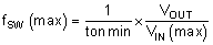
Figure 8-2 shows the maximum recommended input voltage versus output voltage for each FSEL frequency. This graph uses the maximum minimum on time of 40 ns and includes 10% tolerance on the switching frequency.
 Figure 8-2 Maximum Input Voltage vs Output Voltage