SLUSEO6B may 2023 – july 2023 TPSM843B22
PRODUCTION DATA
- 1
- 1 Features
- 2 Applications
- 3 Description
- 4 Revision History
- 5 Pin Configuration and Functions
- 6 Specifications
-
7 Detailed Description
- 7.1 Overview
- 7.2 Functional Block Diagram
- 7.3
Feature Description
- 7.3.1 VIN Pins and VIN UVLO
- 7.3.2 Internal Bypassing (BP5)
- 7.3.3 Enable and Adjustable UVLO
- 7.3.4 Switching Frequency Selection
- 7.3.5 Switching Frequency Synchronization to an External Clock
- 7.3.6 Remote Sense Amplifier and Adjusting the Output Voltage
- 7.3.7 Loop Compensation Guidelines
- 7.3.8 Soft Start and Prebiased Output Start-up
- 7.3.9 MSEL Pin
- 7.3.10 Power Good (PG)
- 7.3.11 Output Overload Protection
- 7.3.12 Output Overvoltage and Undervoltage Protection
- 7.3.13 Overtemperature Protection
- 7.3.14 Output Voltage Discharge
- 7.4 Device Functional Modes
-
8 Application and Implementation
- 8.1 Application Information
- 8.2
Typical Applications
- 8.2.1
1.0-V Output, 1-MHz Application
- 8.2.1.1 Design Requirements
- 8.2.1.2
Detailed Design Procedure
- 8.2.1.2.1 Switching Frequency
- 8.2.1.2.2 Output Inductor Selection
- 8.2.1.2.3 Output Capacitor
- 8.2.1.2.4 Input Capacitor
- 8.2.1.2.5 Adjustable Undervoltage Lockout
- 8.2.1.2.6 Output Voltage Resistors Selection
- 8.2.1.2.7 Bootstrap Capacitor Selection
- 8.2.1.2.8 BP5 Capacitor Selection
- 8.2.1.2.9 PG Pullup Resistor
- 8.2.1.2.10 Current Limit Selection
- 8.2.1.2.11 Soft-Start Time Selection
- 8.2.1.2.12 Ramp Selection and Control Loop Stability
- 8.2.1.2.13 MSEL Pin
- 8.2.1.3 Application Curves
- 8.2.1
1.0-V Output, 1-MHz Application
- 8.3 Power Supply Recommendations
- 8.4 Layout
- 9 Device and Documentation Support
- 10Mechanical, Packaging, and Orderable Information
Package Options
Mechanical Data (Package|Pins)
- RDG|25
Thermal pad, mechanical data (Package|Pins)
Orderable Information
8.2.1.2.12 Ramp Selection and Control Loop Stability
The MSEL pin is used to select between three different ramp settings. The most optimal ramp setting depends on VOUT, fSW, LOUT, and COUT. To get started, calculate LC double pole frequency using Equation 25. Then calculate the ratio between fSW and fLC. Based on this ratio and the output voltage, select the recommended ramp setting using Figure 8-3. With a 1-V output, TI recommends the 1-pF ramp for ratios between approximately 35 and 58, TI recommends the 2-pF ramp for ratios between approximately 58 and 86, and TI recommends the 4-pF ramp for ratios greater than approximately 86. In general, use the largest ramp capacitor the design can support. Increasing the ramp capacitor improves transient response but can reduce stability margin or increase on-time jitter.
For this design, fLC is 15.1 kHz and the ratio is 66.2 which is on the border of the 1-pF and 2-pF ramp settings. Through bench evaluation, it was found the design had sufficient stability margin with the 2-pF ramp so this setting was selected for the best transient response. The recommended ramp settings given by Figure 8-3 include margin to account for potential component tolerances and variations across operating conditions so it is possible to use a higher ramp setting as shown in this example.
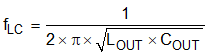
 Figure 8-3 Recommended Ramp Settings
Use a feedforward capacitor (CFF) in parallel with the upper feedback resistor (RFBT) to add a zero into the control loop to provide phase boost. Include a placeholder for this capacitor as the zero it provides can be required to meet phase margin requirements. This capacitor also adds a pole at a higher frequency than the zero. The pole and zero frequency are not independent so as a result, after the zero location is chosen, the pole is fixed as well. The zero is placed at 1 / 4 the fSW by calculating the value of CFF with Equation 26. The calculated value is 64 pF — round this down to the closest standard value of 56 pF.
Using bench measurements of the AC response, the feedforward capacitor for this example design was increased to 100 pF to improve the transient response.
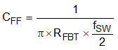
Using larger feedforward capacitors to further improve the transient response is possible, but take care to ensure there is a minimum of –9-dB gain margin in all operating conditions. The feedforward capacitor injects noise on the output into the FB pin. This added noise can result in increased on-time jitter at the switching node. Too little gain margin can cause a repeated wide and narrow pulse behavior. Adding a 100-Ω resistor in series with the feedforward capacitor can help reduce the impact of noise on the FB pin in case of non-ideal PCB layout. The value of this resistor must be kept small as larger values bring the feedforward pole and zero closer together degrading the phase boost the feedforward capacitor provides.
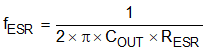
When using higher ESR output capacitors, such as polymer or tantalum, their ESR zero (fESR) must be accounted for. The ESR zero can be calculated using Equation 27. If the ESR zero frequency is less than the estimated bandwidth of 1/10th the fSW, it can affect the gain margin and phase margin. A series R-C from the FB pin to ground can be used to add a pole into the control loop if necessary. All ceramic capacitors are used in this design so the effect of the ESR zero is ignored.