SLVSEJ2A February 2018 – April 2018 TPSM84424
PRODUCTION DATA.
- 1 Features
- 2 Applications
- 3 Description
- 4 Revision History
- 5 Pin Configuration and Functions
- 6 Specifications
-
7 Detailed Description
- 7.1 Overview
- 7.2 Functional Block Diagram
- 7.3
Feature Description
- 7.3.1 Adjusting the Output Voltage
- 7.3.2 Switching Frequency (RT)
- 7.3.3 Synchronization (CLK)
- 7.3.4 Output On/Off Enable (EN)
- 7.3.5 Input Capacitor Selection
- 7.3.6 Output Capacitor Selection
- 7.3.7 TurboTrans (TT)
- 7.3.8 Undervoltage Lockout (UVLO)
- 7.3.9 Soft Start (SS/TR)
- 7.3.10 Sequencing (SS/TR)
- 7.3.11 Power Good (PGOOD)
- 7.3.12 Safe Start-up into Pre-Biased Outputs
- 7.3.13 Overcurrent Protection
- 7.3.14 Thermal Shutdown
- 7.4 Device Functional Modes
- 8 Application and Implementation
- 9 Power Supply Recommendations
- 10Layout
- 11Device and Documentation Support
- 12Mechanical, Packaging, and Orderable Information
Package Options
Mechanical Data (Package|Pins)
- MOL|24
Thermal pad, mechanical data (Package|Pins)
Orderable Information
7.3.4 Output On/Off Enable (EN)
The EN pin provides electrical ON/OFF control of the device. Once the EN pin voltage exceeds the threshold voltage, the device starts operation. If the EN pin voltage is pulled below the threshold voltage, the regulator stops switching and enters low operating current state. The EN pin has an internal pullup current source allowing the user to float the EN pin for enabling the device.
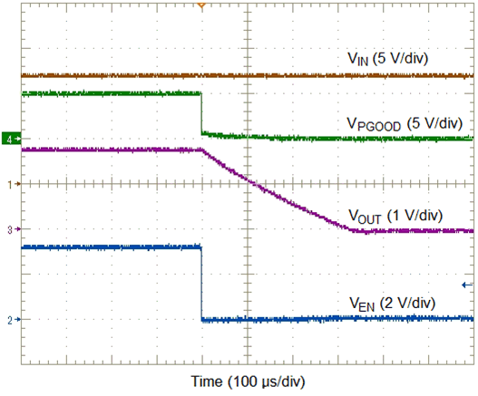
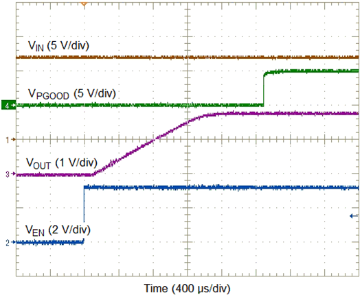
If an application requires controlling the EN pin, either drive it directly with a logic input or use an open drain/collector device to interface with the pin. Applying a low voltage to the enable control (EN) pin disables the output of the supply, shown in Figure 12. When the EN pin voltage exceeds the threshold voltage, the supply executes a soft-start power-up sequence, as shown in Figure 13.
 Figure 12. Enable Turnoff
  Figure 13. Enable Turnon