SLVSEJ3B February   2018  – April 2018 TPSM84624

PRODUCTION DATA.  

  1. Features
  2. Applications
    1.     Simplified Schematic
  3. Description
    1.     Transient Response
  4. Revision History
  5. Pin Configuration and Functions
    1.     Pin Functions
  6. Specifications
    1. 6.1 Absolute Maximum Ratings
    2. 6.2 ESD Ratings
    3. 6.3 Recommended Operating Conditions
    4. 6.4 Thermal Information
    5. 6.5 Electrical Characteristics
    6. 6.6 Switching Characteristics
    7. 6.7 Typical Characteristics (VIN = 12 V)
    8. 6.8 Typical Characteristics (VIN = 5 V)
  7. Detailed Description
    1. 7.1 Overview
    2. 7.2 Functional Block Diagram
    3. 7.3 Feature Description
      1. 7.3.1  Adjusting the Output Voltage
      2. 7.3.2  Switching Frequency (RT)
      3. 7.3.3  Synchronization (CLK)
      4. 7.3.4  Output On/Off Enable (EN)
      5. 7.3.5  Input Capacitor Selection
      6. 7.3.6  Output Capacitor Selection
      7. 7.3.7  TurboTrans (TT)
        1. 7.3.7.1 Low-ESR Output Capacitors
        2. 7.3.7.2 Transient Response
          1. 7.3.7.2.1 Transient Waveforms (VIN = 12 V)
      8. 7.3.8  Undervoltage Lockout (UVLO)
      9. 7.3.9  Soft Start (SS/TR)
      10. 7.3.10 Sequencing (SS/TR)
      11. 7.3.11 Power Good (PGOOD)
      12. 7.3.12 Safe Start-Up Into Pre-Biased Outputs
      13. 7.3.13 Overcurrent Protection
      14. 7.3.14 Thermal Shutdown
    4. 7.4 Device Functional Modes
      1. 7.4.1 Active Mode
      2. 7.4.2 Shutdown Mode
  8. Application and Implementation
    1. 8.1 Application Information
    2. 8.2 Typical Application
      1. 8.2.1 Design Requirements
      2. 8.2.2 Detailed Design Procedure
        1. 8.2.2.1 Custom Design With WEBENCH® Tools
        2. 8.2.2.2 Output Voltage Setpoint
        3. 8.2.2.3 Setting the Switching Frequency
        4. 8.2.2.4 Input Capacitors
        5. 8.2.2.5 Output Capacitors
        6. 8.2.2.6 TurboTrans Resistor
        7. 8.2.2.7 Application Waveforms
  9. Power Supply Recommendations
  10. 10Layout
    1. 10.1 Layout Guidelines
    2. 10.2 Layout Examples
    3. 10.3 EMI
      1. 10.3.1 EMI Plots
    4. 10.4 Package Specifications
  11. 11Device and Documentation Support
    1. 11.1 Device Support
      1. 11.1.1 Third-Party Products Disclaimer
    2. 11.2 Custom Design With WEBENCH® Tools
    3. 11.3 Receiving Notification of Documentation Updates
    4. 11.4 Community Resources
    5. 11.5 Trademarks
    6. 11.6 Electrostatic Discharge Caution
    7. 11.7 Glossary
  12. 12Mechanical, Packaging, and Orderable Information
    1. 12.1 Tape and Reel Information

Package Options

Mechanical Data (Package|Pins)
Thermal pad, mechanical data (Package|Pins)
Orderable Information

Typical Characteristics (VIN = 5 V)

TA = 25°C, unless otherwise noted.
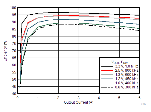
TPSM84624 D007_5V6AEff.gif
Figure 7. Efficiency vs Output Current
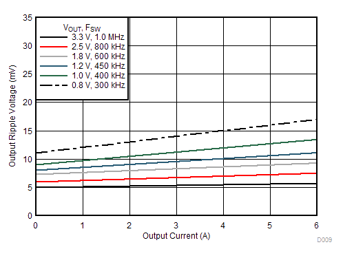
TPSM84624 D009_5V6ARipple.gif
VOUT = 1.2 V fSW = 450 kHz
Figure 9. Ripple Voltage vs Output Current
TPSM84624 D011_3V3SOA.gif
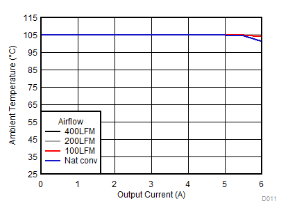
VOUT = 3.3 V fSW = 1 MHz
Figure 11. Safe Operating Area
TPSM84624 D008_5V6APdis.gif
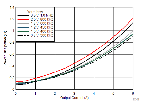
Figure 8. Power Dissipation vs Output Current
TPSM84624 D010_LTE1V8SOA.gif
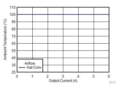
VOUT ≤ 1.8 V
Figure 10. Safe Operating Area