SLVSE06B January 2018 – JANUARY 2019 TPSM846C24
PRODUCTION DATA.
- 1 Features
- 2 Applications
- 3 Description
- 4 Revision History
- 5 Pin Configuration and Functions
- 6 Specifications
-
7 Detailed Description
- 7.1 Overview
- 7.2 Functional Block Diagram
- 7.3
Feature Description
- 7.3.1 Minimum Capacitance Requirements
- 7.3.2 Setting the Compensation Network
- 7.3.3 Transient Response
- 7.3.4 Setting the Output Voltage
- 7.3.5 Differential Remote Sense
- 7.3.6 Switching Frequency and Synchronization
- 7.3.7 Prebiased Output Start-Up
- 7.3.8 Power-Good (PGOOD) Indicator
- 7.3.9 Linear Regulators BP3 and BP6
- 7.3.10 Parallel Application
- 7.3.11 Parallel Operation
- 7.3.12 Overtemperature Protection
- 7.3.13 Overcurrent Protection
- 7.3.14 Output Overvoltage and Undervoltage Protection
- 7.4 Device Functional Modes
- 8 Application and Implementation
- 9 Power Supply Recommendations
- 10Layout
- 11Device and Documentation Support
- 12Mechanical, Packaging, and Orderable Information
Package Options
Mechanical Data (Package|Pins)
- MOL|59
Thermal pad, mechanical data (Package|Pins)
Orderable Information
7.3.2 Setting the Compensation Network
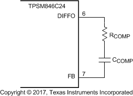
The TPSM846C24 requires an external series resistor and capacitor compensation network to be connected between the DIFFO pin (pin 6) and the FB pin (pin 7). These are RCOMP and CCOMP in Figure 14. The value of these components is determined by the total amount of output capacitance and the switching frequency. TI recommends only ceramic and low-ESR, polymer-type capacitors are. Place these components as close as possible to the module and away from noisy signal traces. Suggested values for RCOMP and CCOMP for some typical values of output capacitance are given in Table 1. Final values should be determined by testing system stability using standard power supply evaluation techniques.
 Figure 14. Compensation Components
 Table 1. Recommended Compensation Components
| TOTAL COUT (µF) | SWITCHING FREQUENCY | TYPICAL COUT | |||||||
|---|---|---|---|---|---|---|---|---|---|
| 300 - 400 kHz | 400 - 600 kHz | 600 - 1000 kHz | |||||||
| MIN | MAX | RCOMP | CCOMP | RCOMP | CCOMP | RCOMP | CCOMP | Ceramic | Polymer |
| 1000 | 1500 | 1.0 kΩ | 1000 pF | 665 Ω | 1500 pF | 499 Ω | 2200 pF | 4 × 47 µF | 2 × 470 µF |
| 1500 | 3000 | 665 Ω | 1500 pF | 499 Ω | 2200 pF | 249 Ω | 4700 pF | 4 × 47 µF | 4 × 470 µF |
| 3000 | 5000 | 499 Ω | 2200 pF | 249 Ω | 4700 pF | 124 Ω | 6800 pF | 4 × 47 µF | 4 × 1000 µF |