SLVSE26B November 2017 – April 2018 TPSM84824
PRODUCTION DATA.
- 1 Features
- 2 Applications
- 3 Description
- 4 Revision History
- 5 Pin Configuration and Functions
- 6 Specifications
-
7 Detailed Description
- 7.1 Overview
- 7.2 Functional Block Diagram
- 7.3
Feature Description
- 7.3.1 Adjusting the Output Voltage
- 7.3.2 Switching Frequency (RT)
- 7.3.3 Synchronization (CLK)
- 7.3.4 Output On/Off Enable (EN)
- 7.3.5 Input Capacitor Selection
- 7.3.6 Output Capacitor Selection
- 7.3.7 TurboTrans (TT)
- 7.3.8 Undervoltage Lockout (UVLO)
- 7.3.9 Soft Start (SS/TR)
- 7.3.10 Sequencing (SS/TR)
- 7.3.11 Power Good (PGOOD)
- 7.3.12 Safe Start-up into Pre-Biased Outputs
- 7.3.13 Overcurrent Protection
- 7.3.14 Thermal Shutdown
- 7.4 Device Functional Modes
- 8 Application and Implementation
- 9 Power Supply Recommendations
- 10Layout
- 11Device and Documentation Support
- 12Mechanical, Packaging, and Orderable Information
Package Options
Mechanical Data (Package|Pins)
- MOL|24
Thermal pad, mechanical data (Package|Pins)
Orderable Information
7.3.8 Undervoltage Lockout (UVLO)
The TPSM84824 implements internal UVLO circuitry on the VIN pin. The device is disabled when the VIN pin voltage falls below the internal VIN UVLO threshold. The internal VIN UVLO rising threshold is 4.1 V (typical) with a typical hysteresis of 200 mV.
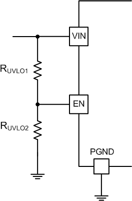
Applications may require a higher UVLO threshold to prevent early turnon, for sequencing requirements, or to prevent input current draw at lower input voltages. An external resistor divider can be added to the EN pin to adjust the UVLO threshold higher. The external resistor divider can be configured as shown in Figure 21. Table 9 lists standard values for RUVLO1 and RUVLO2 to adjust the UVLO voltage higher.
 Figure 21. Adjustable UVLO
 Table 9. Standard Resistor Values for Adjusting UVLO
| VIN UVLO (V) | 4.5 | 5 | 6 | 7 | 8 | 9 | 10 | 11 | 12 |
|---|---|---|---|---|---|---|---|---|---|
| RUVLO1 (kΩ) | 68.1 | 68.1 | 68.1 | 68.1 | 68.1 | 68.1 | 68.1 | 68.1 | 68.1 |
| RUVLO2 (kΩ) | 24.3 | 21.5 | 16.9 | 14 | 12.1 | 10.5 | 9.31 | 8.45 | 7.50 |
| Hysteresis (mV) | 385 | 400 | 430 | 465 | 500 | 530 | 565 | 600 | 640 |