SLVSFQ9A August 2021 – November 2021 TPSM8A28 , TPSM8A29
PRODUCTION DATA
- 1 Features
- 2 Applications
- 3 Description
- 4 Revision History
- 5 Pin Configuration and Functions
- 6 Specifications
-
7 Detailed Description
- 7.1 Overview
- 7.2 Functional Block Diagram
- 7.3
Feature Description
- 7.3.1 Internal VCC LDO and Using External Bias on VCC Pin
- 7.3.2 Enable
- 7.3.3 Output Voltage Setting
- 7.3.4 Internal Fixed Soft Start and External Adjustable Soft Start
- 7.3.5 External REFIN for Output Voltage Tracking
- 7.3.6 Frequency and Operation Mode Selection
- 7.3.7 D-CAP3™ Control
- 7.3.8 Low-Side FET Zero-Crossing
- 7.3.9 Current Sense and Positive Overcurrent Protection
- 7.3.10 Low-Side FET Negative Current Limit
- 7.3.11 Power Good
- 7.3.12 Overvoltage and Undervoltage Protection
- 7.3.13 Out-Of-Bounds (OOB) Operation
- 7.3.14 Output Voltage Discharge
- 7.3.15 UVLO Protection
- 7.3.16 Thermal Shutdown
- 7.4 Device Functional Modes
-
8 Application and Implementation
- 8.1 Application Information
- 8.2
Typical Application
- 8.2.1 Design Requirements
- 8.2.2
Detailed Design Procedure
- 8.2.2.1 Output Voltage Setting Point
- 8.2.2.2 Choose the Inductor
- 8.2.2.3 Set the Current Limit (TRIP)
- 8.2.2.4 Choose the Output Capacitor
- 8.2.2.5 Choose the Input Capacitors (CIN)
- 8.2.2.6 Soft-Start Capacitor (SS/REFIN Pin)
- 8.2.2.7 EN Pin Resistor Divider
- 8.2.2.8 VCC Bypass Capacitor
- 8.2.2.9 BOOT Capacitor
- 8.2.2.10 PGOOD Pullup Resistor
- 8.2.3 Application Curves
- 9 Power Supply Recommendations
- 10Layout
- 11Device and Documentation Support
- 12Mechanical, Packaging, and Orderable Information
Package Options
Mechanical Data (Package|Pins)
- RDG|25
Thermal pad, mechanical data (Package|Pins)
Orderable Information
7.3.9 Current Sense and Positive Overcurrent Protection
For a buck converter, during the on time of the high-side FET, the switch current increases at a linear rate determined by the following:
- input voltage
- output voltage
- the on time
- the output inductor value
During the on time of the low-side FET, this current decreases linearly. The average value of the switch current equals to the load current.
The output overcurrent limit (OCL) is implemented using a cycle-by-cycle valley current detect control circuit. The inductor current is monitored during the on time of the low-side FET by measuring the low-side FET drain-to-source current. If the measured drain-to-source current of the low-side FET is above the current limit threshold, the low-side FET stays ON until the current level becomes lower than the current limit threshold. This type of behavior reduces the average output current sourced by the device. During an overcurrent condition, the current to the load exceeds the current to the output capacitors. Thus, the output voltage tends to decrease. Eventually, when the output voltage falls below the undervoltage-protection threshold (80%), the UVP comparator detects it and shuts down the device after a wait time of 68 µs. The device then enters a hiccup sleep period for approximately 14 ms. After this waiting period, the device attempts to start up again/remains latched off state (both high-side and low-side FETs are latched off) until a reset of VIN or a re-toggling on the EN pin. Figure 7-3 shows the cycle-by-cycle valley current limit behavior as well as the wait time before the device shuts down.
If an OCL condition happens during start-up, the device still has cycle-by-cycle current limit based on low-side valley current. After soft start is finished, the UV event, which is caused by the OC event, shuts down the device and enters Hiccup mode with a wait time of 68 µs.
The resistor, RTRIP, connected from the TRIP pin to AGND sets current limit threshold. ±1% tolerance resistor is highly recommended because a worse tolerance resistor provides less accurate OCL threshold.
To protect the device from unexpected connection on the TRIP pin, an internal fixed OCL clamp is implemented. This internal OCL clamp limits the maximum valley current on LS FET when TRIP pin has too small resistance to AGND, or is accidently shorted to ground.
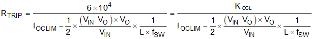
where
- IOCLIM is overcurrent limit threshold for load current in A
- RTRIP is TRIP resistor value in Ω
- VIN is input voltage value in V
- VO is output voltage value in V
- L is output inductor value in µH
- fSW is switching frequency in MHz
 Figure 7-3 Overcurrent Protection