SLVSFQ9A August 2021 – November 2021 TPSM8A28 , TPSM8A29
PRODUCTION DATA
- 1 Features
- 2 Applications
- 3 Description
- 4 Revision History
- 5 Pin Configuration and Functions
- 6 Specifications
-
7 Detailed Description
- 7.1 Overview
- 7.2 Functional Block Diagram
- 7.3
Feature Description
- 7.3.1 Internal VCC LDO and Using External Bias on VCC Pin
- 7.3.2 Enable
- 7.3.3 Output Voltage Setting
- 7.3.4 Internal Fixed Soft Start and External Adjustable Soft Start
- 7.3.5 External REFIN for Output Voltage Tracking
- 7.3.6 Frequency and Operation Mode Selection
- 7.3.7 D-CAP3™ Control
- 7.3.8 Low-Side FET Zero-Crossing
- 7.3.9 Current Sense and Positive Overcurrent Protection
- 7.3.10 Low-Side FET Negative Current Limit
- 7.3.11 Power Good
- 7.3.12 Overvoltage and Undervoltage Protection
- 7.3.13 Out-Of-Bounds (OOB) Operation
- 7.3.14 Output Voltage Discharge
- 7.3.15 UVLO Protection
- 7.3.16 Thermal Shutdown
- 7.4 Device Functional Modes
-
8 Application and Implementation
- 8.1 Application Information
- 8.2
Typical Application
- 8.2.1 Design Requirements
- 8.2.2
Detailed Design Procedure
- 8.2.2.1 Output Voltage Setting Point
- 8.2.2.2 Choose the Inductor
- 8.2.2.3 Set the Current Limit (TRIP)
- 8.2.2.4 Choose the Output Capacitor
- 8.2.2.5 Choose the Input Capacitors (CIN)
- 8.2.2.6 Soft-Start Capacitor (SS/REFIN Pin)
- 8.2.2.7 EN Pin Resistor Divider
- 8.2.2.8 VCC Bypass Capacitor
- 8.2.2.9 BOOT Capacitor
- 8.2.2.10 PGOOD Pullup Resistor
- 8.2.3 Application Curves
- 9 Power Supply Recommendations
- 10Layout
- 11Device and Documentation Support
- 12Mechanical, Packaging, and Orderable Information
Package Options
Mechanical Data (Package|Pins)
- RDG|25
Thermal pad, mechanical data (Package|Pins)
Orderable Information
7.4.1 Auto-Skip Eco-Mode Light Load Operation
While the MODE pin is pulled to VCC directly or connected to AGND pin through a resistor larger than 121 kΩ, the device automatically reduces the switching frequency at light-load conditions to maintain high efficiency. This section describes the operation in detail.
As the output current decreases from heavy load condition, the inductor current also decreases until the rippled valley of the inductor current touches zero level. Zero level is the boundary between the continuous-conduction and discontinuous-conduction modes. The synchronous MOSFET turns off when this zero inductor current is detected. As the load current decreases further, the converter runs into discontinuous-conduction mode (DCM). The on time is maintained to a level approximately the same as during continuous-conduction mode operation so that discharging the output capacitor with a smaller load current to the level of the reference voltage requires more time. The transition point to the light-load operation IO(LL) (for example: the threshold between continuous- and discontinuous-conduction mode) is calculated as shown in Equation 6.
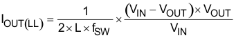
where
- fSW is the switching frequency
Using only ceramic capacitors is recommended for Skip mode.